Ion-beam deposition process for manufacturing multi-layered attenuated phase shift photomask blanks

a phase shift photomask and photomask technology, which is applied in the direction of originals for photomechanical treatment, instruments, vacuum evaporation coating, etc., can solve the problems of etching or removal of film, inability to accurately control the process of sputtering plasma, and limited resolution for imaging the minimum feature size on the wafer with a particular wavelength of ligh

Inactive Publication Date: 2004-06-17
EI DU PONT DE NEMOURS & CO
View PDF12 Cites 11 Cited by
  • Summary
  • Abstract
  • Description
  • Claims
  • Application Information

AI Technical Summary

Problems solved by technology

However, as the feature size decreases, resolution for imaging the minimum feature size on the wafer with a particular wavelength of light is limited by the diffraction of light.
Furthermore, the IBD process has the ability to independently control the deposition flux and the reactive gas ion flux (current) and energy, which are coupled and not independently controllable in planar magnetron sputtering.
While magnetron sputtering is extensively used in the electronics industry for reproducibly depositing all sorts of coatings, process control in sputtering plasmas is not accurate because the direction, energy, and flux of the ions incident on the growing film cannot be regulated.
For the "assist" ions, lower energy typically <500 eV are preferred, otherwise the ions may cause undesirable etching or removal of the film.
While it is possible to make films with complex chemistry such as Si.sub.3N.sub.4, with ion beam deposition using a single ion source the process is more restrictive than for dual ion beam deposition.
Huang et al. in "Structure and composition studies for silicon nitride thin films deposited by single ion beam sputter deposition" Thin Solid Films 299 (1997) 104-109, demonstrated that films with Si.sub.3N.sub.4 properties only form when the beam voltage is in a narrow range about 800 V. Although a nitride target can be used at the outset with a single ion source to improve process latitude, the deposition rate can be impracticably slow and the purity of a nitride target is generally inferior to an elemental target.

Method used


Image

  • Ion-beam deposition process for manufacturing multi-layered attenuated phase shift photomask blanks
  • Ion-beam deposition process for manufacturing multi-layered attenuated phase shift photomask blanks
  • Ion-beam deposition process for manufacturing multi-layered attenuated phase shift photomask blanks

Examples


examples 1 and 2

SiN / TiN Multilayers

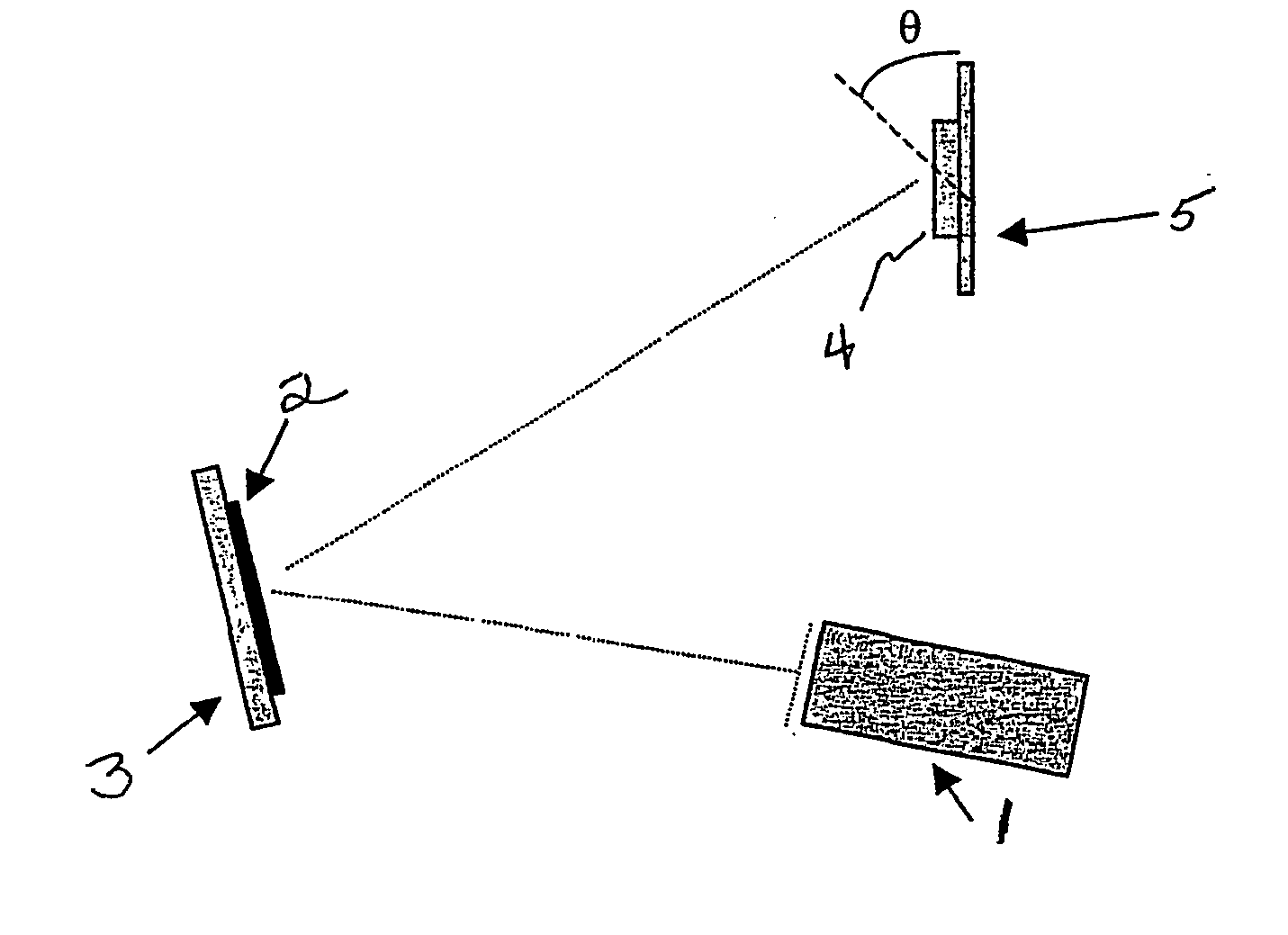
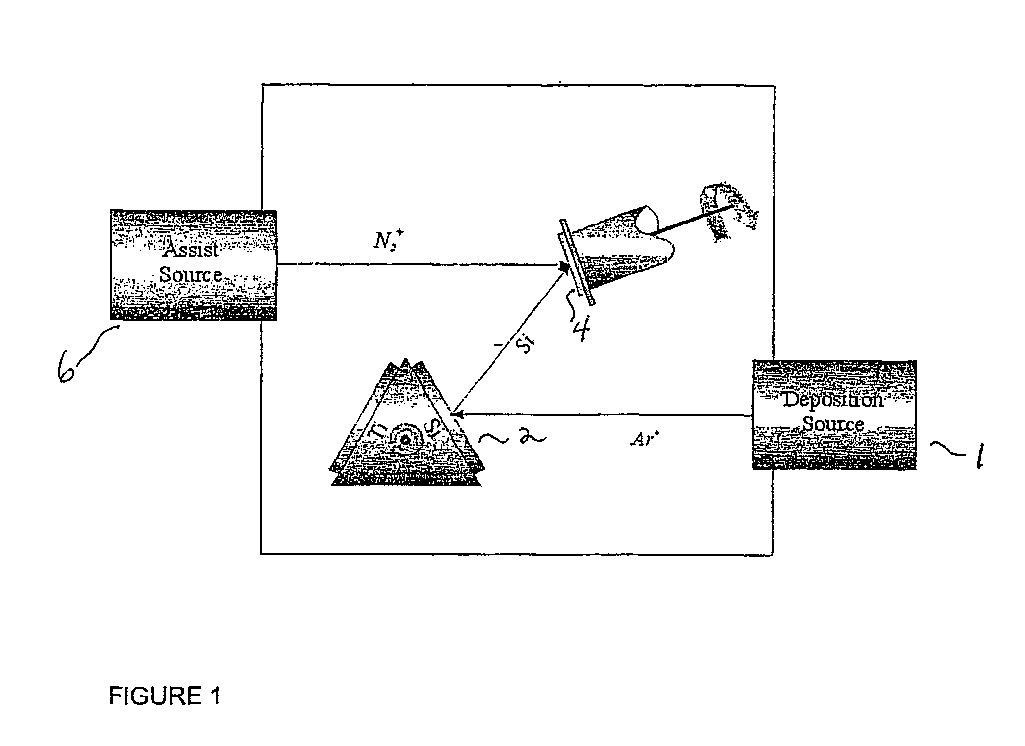
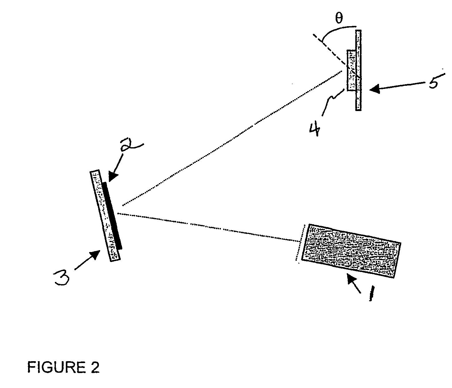
[0045] TiN / SiN multilayers were made by dual ion beam deposition in a Veeco IBD-210 apparatus from a Si and a Ti target. Alternate deposition from Ti and Si was carried out with the deposition source operating at a voltage of 750 V and a beam current of 160 mA. Ar gas of 6 sccm was delivered to the deposition source. Nitride formation in the growing film on the substrate was accomplished by bombarding the film with nitrogen ions from a separate ion assist source operating at 50 V and a current of 20 mA with nitrogen at 8 sccm delivered to the assist source. The substrate was 6.times.6-inch square quartz plate, with a thickness of 1 / 4 inch. The following film compositions were synthesized by depositing alternately from Ti and Si targets;

15.times.(1.2 nm TiN+5.68 nm SiN) and (1)

15.times.(1.45 nm TiN+5.43 nm SiN) (2)

[0046] Formula (1) correspond to a multilayer structure of alternating TiN and SiN layers with thickness 1.2 nm (TiN) and 5.68 nm (SiN), respectively. Th...

examples 3 , 4 , 5

Examples 3, 4, 5

SiON / TiON Multilayers

[0048] In these examples, TiON / SiON multilayers were made by dual ion beam deposition in a commercial tool (Veeco IBD-210) from an Si and a Ti target. Adding a small concentration of O.sub.2 to the N.sub.2 in the assist ion source had the effect of increasing the optical transmission for phase-shift mask application at 193 nm, since the optical absorption of the oxynitrides, especially SiON, is less than that for SiN. A higher transmission in a phase-shift mask can enhance the optical contrast or printing resolution. Multilayers of SiON / TiON were synthesized by alternately depositing from Ti and Si targets. The deposition ion beam source was operated at a voltage of 750 V and a beam current of 160 mA, while the assist source with N.sub.2 and O.sub.2 was operated at 50 V and a current of 20 mA. 6 sccm of Ar was delivered to the deposition source, while 6 sccm of N.sub.2 and 2 sccm of a 10% O.sub.2 / 90% N.sub.2 mixture were delivered to the assist s...

example 6

SiN by Single Ion Beam Source (700 V)

[0053] Silicon nitride films were deposited from an Si target on to quartz substrates, 1.5 in..times.1.0 in..times.0.25 in., using a 3 cm commercial (Commonwealth, Inc.) ion beam source, operating at 700 V beam voltage and 25 mA beam current. The deposition gases were 6 sccm N.sub.2 and 1.37 sccm Ar. Two hours of deposition produced a film 580 A thick (4.83 A / min) with an optical transmission at 193 nm of 15.7%, corresponding to an extinction coefficient k=0.39, attractive for phase-shift mask application.


PUM

PropertyMeasurementUnit
lithographic wavelengthsaaaaaaaaaa
optical bandgap energyaaaaaaaaaa
lithographic wavelengthaaaaaaaaaa

Abstract

A single ion-beam deposition, or a dual ion-beam deposition process for fabricating attenuating phase shift photomask blanks capable of producing a phase shift of 180° and having an optical transmissivity of at least 0.001 at selected lithographic wavelengths <400 nm, comprising at least one layer of an optically transmitting and/or one layer of optically absorbing elemental or a compound material in a periodic or an aperiodic arrangement.

Description

[0001] This invention relates to manufacture of phase shift photomask blanks in photolithography, known in the art as the attenuating (embedded) type, using ion-beam deposition techniques. More specifically, this invention relates to attenuating phase-shift photomask blanks to be used with short wavelength (i.e., <400 nanometer) light, which attenuate and change the phase of transmitted light by 180.degree. relative to the incident light. Additionally, this invention relates to photomask blanks with multi-layered coatings of simple or complex compounds of elemental materials on the blanks.TECHNICAL BACKGROUND[0002] Microlithography is the process of transferring microscopic circuit patterns or images, usually through a photomask, on to a silicon wafer. In the production of integrated circuits for computer microprocessors and memory devices, the image of an electronic circuit is projected, usually with an electromagnetic wave source, through a mask or stencil on to a photosensitiv...

Claims


Application Information

Patent Timeline
Patent Type & Authority Applications(United States)
IPC IPC(8): C23C14/00C23C14/06C23C14/46G03F1/32
CPCC23C14/0052C23C14/0641G03F1/32C23C14/46C23C14/0676
Inventor CARCIA, PETER FRANCISDIEU, LAURENT
Owner EI DU PONT DE NEMOURS & CO
Why Eureka
Try Eureka