Micromachined heaters for microfluidic devices

a microfluidic device and heater technology, applied in semiconductor devices, semiconductor/solid-state device details, electrical apparatus, etc., can solve the problems of device burnout, heavy ion implantation is an expensive process, and further increase in current only broadens the active area of heating elements, and achieves low aspect ratio

Inactive Publication Date: 2004-09-16
NEW JERSEY INSTITUTE OF TECHNOLOGY
View PDF11 Cites 19 Cited by
  • Summary
  • Abstract
  • Description
  • Claims
  • Application Information

AI Technical Summary

Benefits of technology

[0012] It is another object of the present invention to provide a microheater device for microfluidic applications in which the heating element allows in-situ heating of the channel only and does not require the heating of the whole chip bulk.
[0028] Now referring to FIG. 1 a preferred embodiment of a method for preparing a microheater 2 for a microfluidic device according to the present invention is disclosed. Wafer 10 may comprise a commercially available material commonly used for photolithographic fabrication such as but not limited to quartz or borosilicate glass. Quartz is a desirable material in electrophoresis because it is a good electrical insulator and is transparent to the UV required for absorbance and fluorescence detection. Quartz substrates also generate high electroosmotic flow rates and have favorable surface characteristics after fabrication by etching. Silicon is also desirable in microfluidic applications because it is possible to embed both fluid-control and fluid detection by integrated circuits on one substrate. By way of comparison the typical fluidic devices such as microreactors and microfluidic capillaries are 2-3 cm.sup.2 in size, and are made of silicon, glass, quartz, or plastic that are either etched, microimprinted or molded. The etched channels and chambers are usually covered with Pyrex, glass or silicon to contain the sample and the reagent. In a preferred embodiment wafer 10 comprises an oriented, p-typed (boron doped), single side polished silicon wafer with a thickness of 575 .mu.m and a resistivity of 10-25-cm.
[0032] Now referring to FIGS. 2A-2E in a preferred embodiment a microheater 2 is formed whereby a conductor 26 is deposited in channel 20 instead of ion implantation as in FIGS. 1D-1E. Referring to FIGS. 2A-2C the identical steps are performed for preparing the wafer 10 and forming channel 20 as in FIGS. 1A-1C. In FIG. 2D, however, deposition of a conductor 26 such as but not limited to a metal in the channel 20 by sputtering is performed. Conductor 26 may be any suitable conducting material such as but not limited to iron, copper, aluminum, chromium, gold, silver, platinum or the like, alloys thereof, composites of organic conducting polymers and metals and the like. Conductor 26 may be substituted by a suitable organic conducting polymer. In a most preferred embodiment the conductor 26 is an aluminum alloy comprising 99% aluminum, the rest being silicon and copper. Silicon-aluminum alloys prevent the silicon from reacting with the deposited aluminum, which could cause spiking or short circuits.

Problems solved by technology

However, heavy ion implantation is an expensive process.
However, once the maximum temperature is reached, any further increase in current only broadens the active area of the heating element.
Thus, continued operation in this region leads to device weakening and eventually device burn out.
To date, however, no microheater that is an integral part of a microchannel has been provided in a microfluidic device.

Method used


Image

  • Micromachined heaters for microfluidic devices
  • Micromachined heaters for microfluidic devices
  • Micromachined heaters for microfluidic devices

Examples


experiment 2

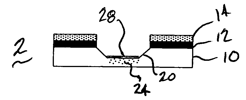
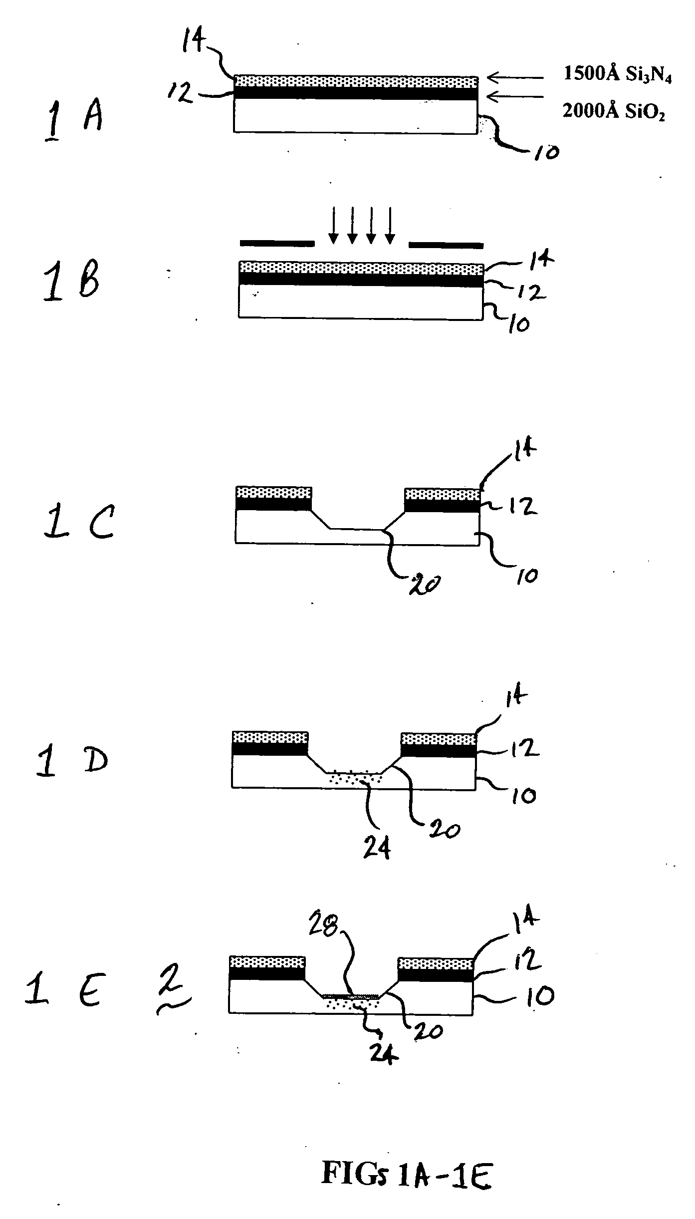
[0039] A set of microheaters was made by low dose boron implantation in accordance with the method of FIGS. 1A-1E. The resistance was a function of dopant concentration. The wafers were annealed at 400.degree. C. in presence of argon. The annealing brought some of the dispersed dopant ions closer to the surface, thus forming a uniform conductive layer. Inadequate annealing could result in a bulk of the implanted ions being distributed too deep into the substrate to contribute to conductivity. Two different implantation regimes were used. Furthermore, in an effort to improve heating characteristics, each was subjected to two different anneal times.

[0040] In order to arrive at the proper energy and dose of the boron source, the concentration following the annealing was simulated using a computer program called SUPREME III (Stanford University Process Emulator). This determined the penetration depth of the boron atoms. For the first run, implantation energy was 80 keV at a dose of 1.ti...

experiment 3

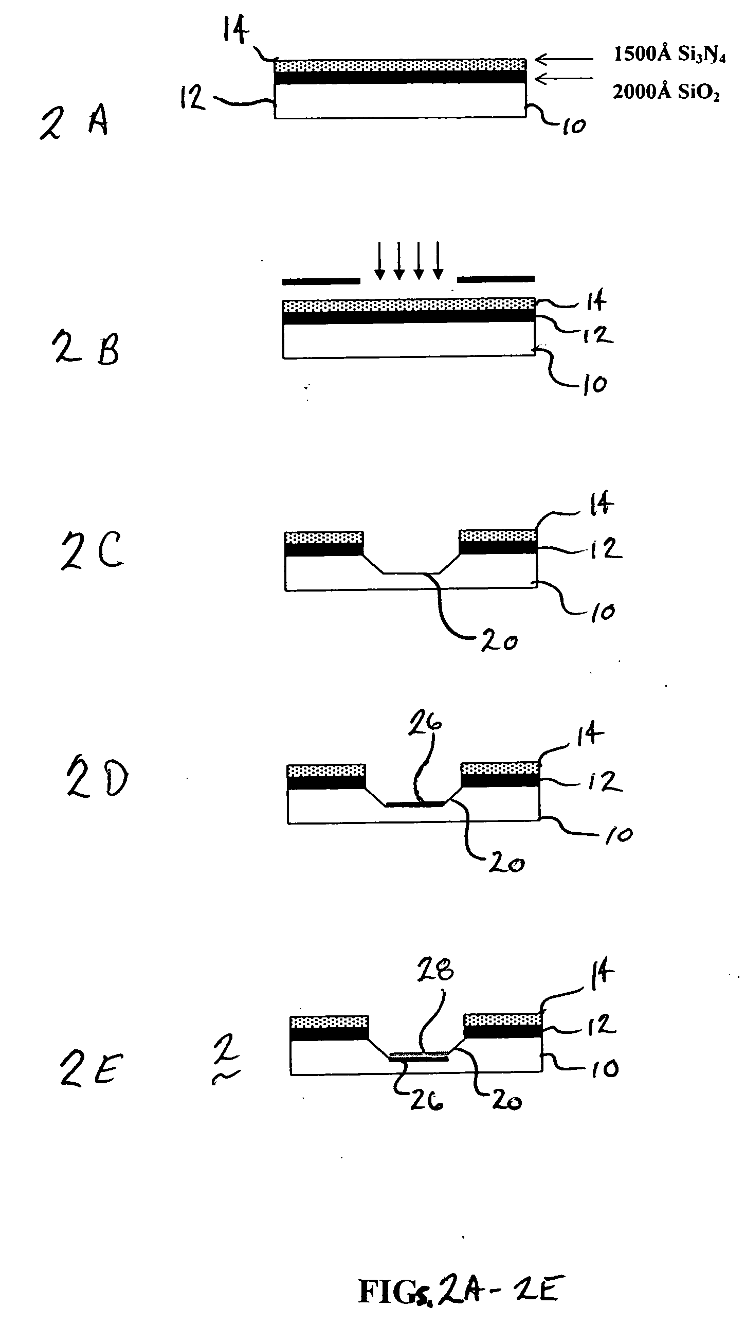
[0044] Effect of Glass Coating SOG was applied on the channels to see how it affected the temperature characteristics. A glass thickness of 1 .mu.m was applied to the microchannels employing aluminum alloy conductors in accordance with FIG. 2E. This was followed by hard plate baking at 80.degree. C., 150.degree. C. and 250.degree. C. for 40 seconds each. Then the wafers were cured in a furnace at 425.degree. C. for 60 minutes.

[0045] The rise in temperature as a function of time with the spin-on glass coating are presented in FIG. 6 which shows temperature characteristics of 1 .mu.m metal deposited heater type A and D with Spin-On-Glass, at an applied voltage of 43 V. In all cases, the temperature stabilized in less than 10 seconds. A thinner glass layer will permit the microheater of the present invention to attain higher temperatures.

[0046] Stability

[0047] It has been found the microchannel heaters of the present invention, especially those having the characteristics of type A in T...


PUM

PropertyMeasurementUnit
temperaturesaaaaaaaaaa
thicknessaaaaaaaaaa

Abstract

Microfabricated heaters for microfluidic devices for lab-on-a-chip applications comprising channels using deposited conductors such as sputtered metal, alloys, polymers and composites thereof; or conductors prepared by ion implantation, and methods for fabricating same are disclosed. Rapid heating to temperatures above 360° C. and rapid cooling is possible using these microheaters. Repeated heating does not lead to the microheater devices weakening or burning out. Preferred embodiments include application of spin-on-glass on the microheater surface.

Description

[0001] This application claims the benefit of U.S. Provisional Application No. 60 / ______, filed Dec. 13, 2002, entitled "Micromachined Heater for Microfluidic Devices," Docket No. 02-05 (PROV) with named inventors Somenath Mitra, Minhee Kim and Durgamadhab Misra, the entirety of which is incorporated herein by reference.[0002] The present invention relates to microheaters, specifically, microheaters for microfluidic devices.[0003] Microfluidic devices are used in various applications such as chemical analysis, reaction engineering, drug discovery, electronics chip cooling, flow sensors and biomedical devices. Microfluidics are also being employed in separation techniques such as gas chromatography, liquid chromatography, and electrophoresis. In fact, it has been demonstrated that it is possible to put a conventional chemical laboratory onto a single microchip to produce large numbers of parallel analysis. Performance enhancement, high throughput, low power consumption, reduction of ...

Claims


Application Information

Patent Timeline
Patent Type & Authority Applications(United States)
IPC IPC(8): H01L23/34
CPCH01L23/345H01L2924/0002H01L2924/00
Inventor MITRA, SOMENATHMISRA, DURGAMADHAB
Owner NEW JERSEY INSTITUTE OF TECHNOLOGY
Why Eureka
Try Eureka