Plasma apparatus, gas distribution assembly for a plasma apparatus and processes therewith

a technology of plasma apparatus and gas distribution assembly, which is applied in the direction of greenhouse gas capture, chemical vapor deposition coating, coating, etc., can solve the problems of limiting the overall chip speed, increasing the dielectric constant, and material loss, and achieves high ashing selectivity

Active Publication Date: 2004-12-02
LAM RES CORP
View PDF76 Cites 198 Cited by
  • Summary
  • Abstract
  • Description
  • Claims
  • Application Information

AI Technical Summary

Benefits of technology

0072] Advantageously, the loadlock chamber provides a mechanism for cooling the substrate to below 100.degree. C. Moreover, the loadlock chamber as described above does not require venting between wafers, which could potentially introduce contaminants to the substrate. As previously discussed, oxygen and nitrogen are detrimental to low k dielectric materials. Eliminating or minimizing contact with these gases is important to maintain the beneficial properties of the low k dielectric material.
0073] Preferably, the plasma apparatus described above is used with substrates, wherein the low k materials contain carbon and/or hydrogen within its structure such as

Problems solved by technology

As integrated devices become smaller, the RC-delay time of signal propagation along interconnects becomes one of the dominant factors limiting overall chip speed.
The ashing step is typically followed by a wet chemical treatment to remove traces of the residue, which can cause further degradation of the low k dielectric, loss of material, and may also cause increase in the dielectric constant.
Although gas mixtures containing one or more of these sources efficiently ash photoresist from the substrate, the use of these gas sources has proven detrimental to substrates containing low k dielectrics.
The increases in dielectric constant affects, among others, interconnect capacitance, which directly impacts device performance.
Moreover, the use of oxygen-containing plasmas is generally less preferred for advanced device fabrication employing copper metal layers since copper metal is readily oxidized.
Occasionally, the damage caused by oxygen containing plasmas is not readily detected during metrology inspection of the substrate after plasma processing.
However, the damage can be readily demonstrated and observed by a subsequent wet cleaning process, as may be typically employed after plasma ashing, wherein portions of the carbon and/or hydrogen-containing low k dielectric material are removed.
The removed portions of the dielectric material are a source of vari

Method used


Image

  • Plasma apparatus, gas distribution assembly for a plasma apparatus and processes therewith
  • Plasma apparatus, gas distribution assembly for a plasma apparatus and processes therewith
  • Plasma apparatus, gas distribution assembly for a plasma apparatus and processes therewith

Examples


Embodiment Construction

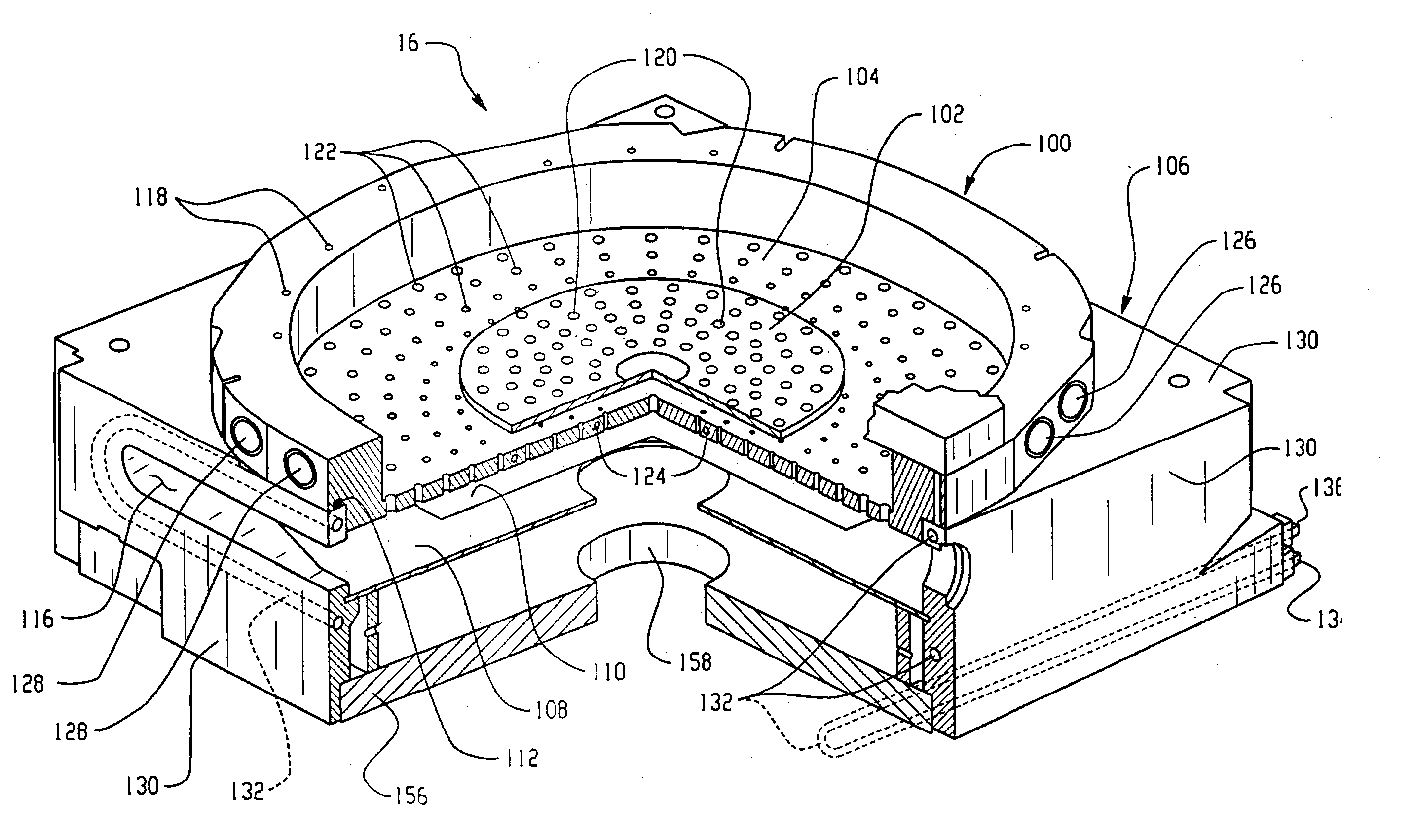
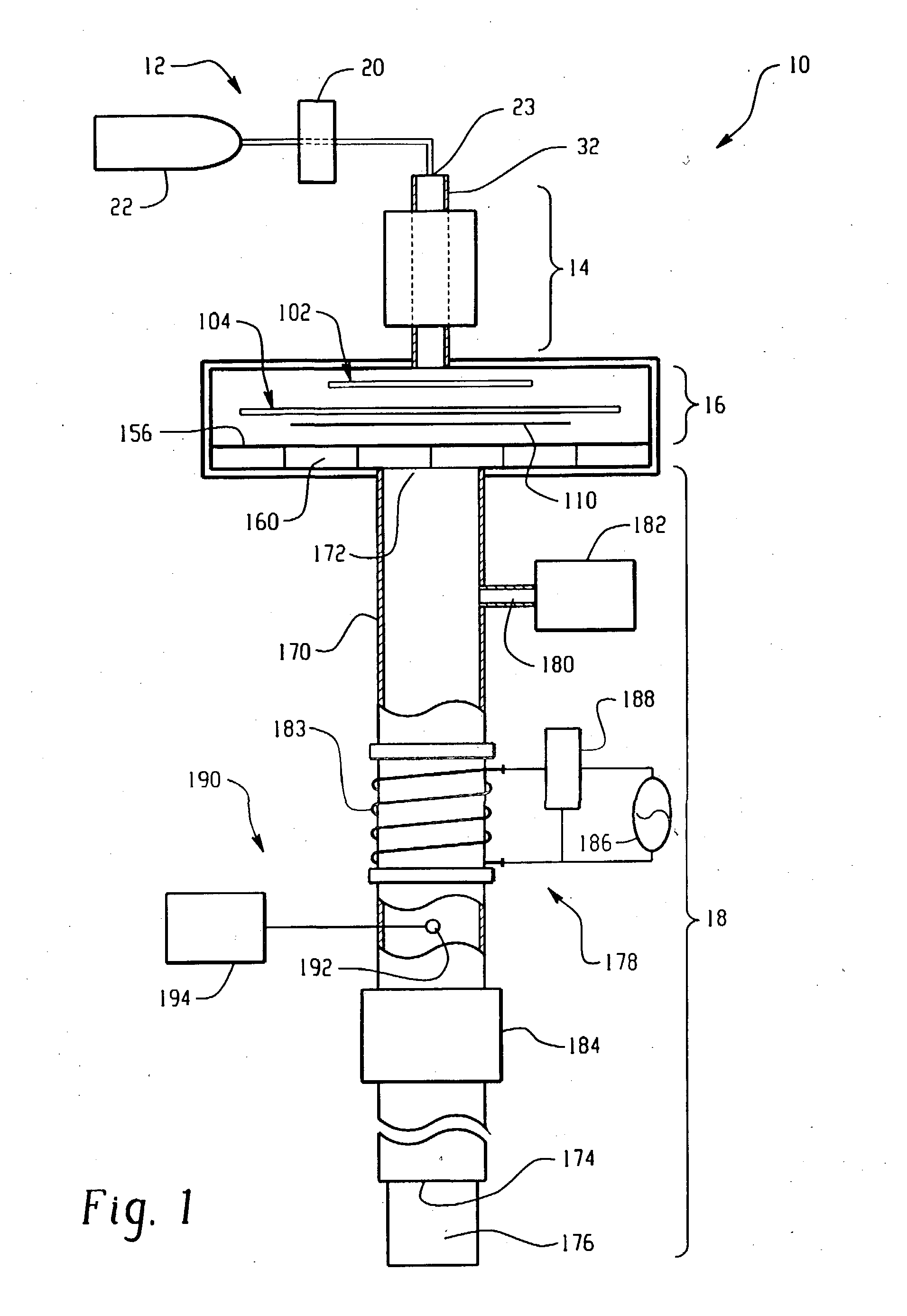
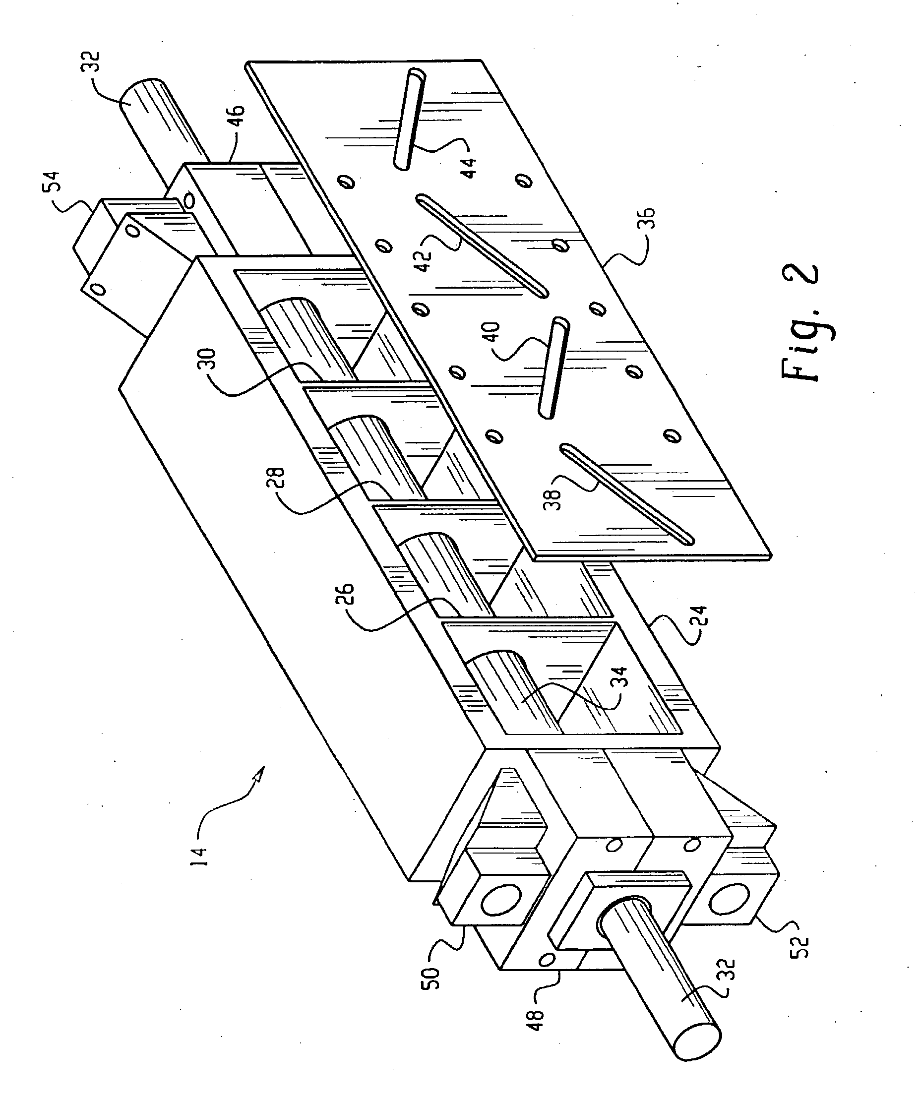
[0084] In this example, plasma uniformity was examined using different dual baffle plate configurations in a Fusion ES3 downstream microwave plasma asher commercially available from the Axcelis Technologies Corporation. Multiple 300 mm silicon wafers were coated with 0.75 microns of AZ1505 photoresist under identical conditions and exposed to a 4% hydrogen in helium plasma at 1.1 torr at the temperature indicated in Table 1. AZ1505 photoresist is commercially available by the Hoechst Corporation. The upper baffle plates were identical for each configuration. A control lower baffle plate consisting of 420 apertures evenly spaced across a 13" circular area was employed. Each aperture was 0.113 inches in diameter. Plasma uniformity for the control was compared to two different configurations in accordance with the teachings of the present disclosure. Configuration 1 consisted of 570 apertures evenly spaced across a 15-inch circular area. Apertures within a 5-inch radius from the center...


PUM

PropertyMeasurementUnit
Fractionaaaaaaaaaa
Fractionaaaaaaaaaa
Fractionaaaaaaaaaa

Abstract

A plasma apparatus, various components of the plasma apparatus, and an oxygen free and nitrogen free processes for effectively removing photoresist material and post etch residues from a substrate with a carbon and/or hydrogen containing low k dielectric layer(s).

Description

[0001] The present disclosure relates to semiconductor apparatuses and processes, and more particularly, to plasma mediated processes and plasma apparatuses suitable for ashing organic material from a substrate including a low k dielectric material.[0002] Recently, much attention has been focused on developing low k dielectric thin films for use in the next generation of microelectronics. As integrated devices become smaller, the RC-delay time of signal propagation along interconnects becomes one of the dominant factors limiting overall chip speed. With the advent of copper technology, R has been pushed to its practical lowest limit so attention must be focused on reducing C. One way of accomplishing this task is to reduce the average dielectric constant (k) of the thin insulating films surrounding interconnects. The dielectric constant (k) of traditional silicon dioxide insulative materials is about 3.9. Lowering the dielectric constant (k) below 3.9 will provide a reduced capacita...

Claims


Application Information

Patent Timeline
IPC IPC(8): H01J37/32
CPCH01J37/32357H01J37/3244H01J37/32844Y02C20/30H01J37/32
Inventor BECKNELL, ALAN FREDERICKBUCKLEY, THOMAS JAMESFERRIS, DAVIDPINGREE, RICHARD E. JR.SAKTHIVEL, PALANIKUMARANSRIVASTAVA, ASEEM KUMARWALDFRIED, CARLO
Owner LAM RES CORP
Why Eureka
Try Eureka