Solid-state image sensor, production method for solid-state image sensor, and camera using solid-state image sensor

Inactive Publication Date: 2005-01-13
CANON KK
View PDF19 Cites 35 Cited by
  • Summary
  • Abstract
  • Description
  • Claims
  • Application Information

AI Technical Summary

Benefits of technology

Accordingly, an object of the present invention is to provide an inexpensive and high-definition solid-

Problems solved by technology

For this reason, there is a restriction on the gate voltage during a transfer operation for reading signal charges accumulated in a photodiode in each pixel, and it is not always easy to design a transfer structure for the signal charges accumulated in the photodiode.
In particular, when a buried pho

Method used


Image

  • Solid-state image sensor, production method for solid-state image sensor, and camera using solid-state image sensor
  • Solid-state image sensor, production method for solid-state image sensor, and camera using solid-state image sensor
  • Solid-state image sensor, production method for solid-state image sensor, and camera using solid-state image sensor

Examples


Example

[First Embodiment]

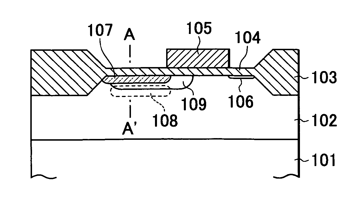
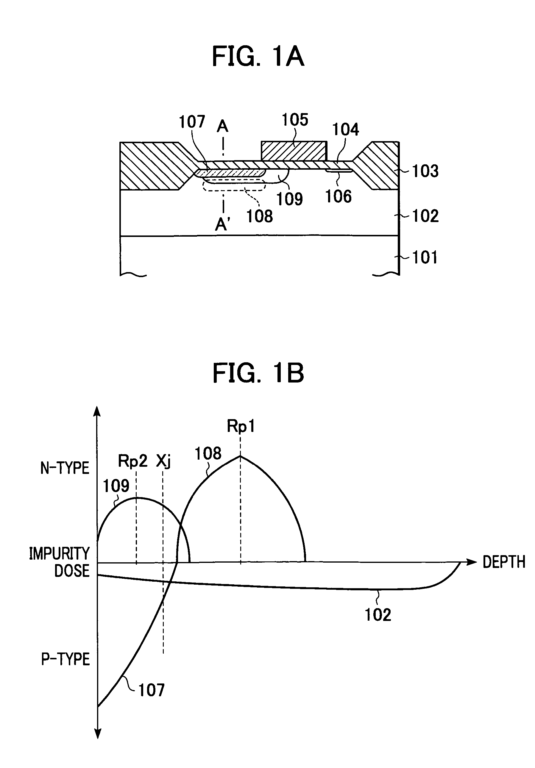
FIG. 1A is an explanatory view of a solid-state image sensor according to a first embodiment of the present invention, and FIG. 1B is a graph showing an impurity concentration distribution at a cross section taken along line A-A′ in FIG. 1A.

Referring to FIG. 1A, a solid-state image sensor of the first embodiment includes, in each pixel, a semiconductor substrate 101, a p-type well region 102, a selective oxide 103, a gate oxide 104, and a transfer gate 105. By turning the transfer gate 105 on, charges in a photodiode are read into an n-type diffusing region 106. The photodiode is of a buried type including a front p-type high-concentration layer 107, an n-type deep accumulation region 108, and an n-type shallow accumulation region 109. Unlike the shallow accumulation region 109, the deep accumulation region 108 does not extend up toward the transfer gate 105. That is, an impurity region of the shallow accumulation region 109 is provided adjacent to the transfer ...

Example

[Second Embodiment]

While the deep accumulation region and the shallow accumulation region in the photodiode are formed by phosphorus implantation in the first embodiment, a deep accumulation region in a photodiode may be formed by arsenic implantation, as in a second embodiment.

The second embodiment of the present invention will be described with reference to FIG. 4. A solid-state image sensor of the second embodiment includes, in each pixel, a semiconductor substrate 401, a p-type well region 402, a selective oxide 403, a gate oxide 404, and a transfer gate 405. By turning the transfer gate 405 on, charges in a photodiode are read into an n-type diffusion region 406. The photodiode is of a buried type, including a front p-type high-concentration layer 407, an n-type deep accumulation region 408, and an n-type shallow accumulation region 409. In the second embodiment, the deep accumulation region 408 is formed by arsenic implantation. Since arsenic has a thermal diffusion consta...

Example

[Third Embodiment]

While the deep accumulation region and the shallow accumulation region in the photodiode are formed by phosphorus implantation in the first embodiment, a shallow accumulation region of a photodiode may be formed by arsenic implantation, as in a third embodiment.

The third embodiment of the present invention will be described with reference to FIG. 5. Referring to FIG. 5, a solid-state image sensor of the third embodiment includes, in each pixel, a semiconductor substrate 501, a p-type well region 502, a selective oxide 503, a gate oxide 504, and a transfer gate 505. By turning the transfer gate 505 on, charges in a photodiode are read into an n-type diffusion region 506. The photodiode is of a buried type including a front p-type high-concentration layer 507, an n-type deep accumulation region 508, and an n-type shallow accumulation region 509. In the third embodiment, the shallow accumulation region 509 is formed by arsenic implantation. Since the thermal diffu...


PUM


Abstract

A solid-state image sensor includes, in each pixel, a p-type well provided on a semiconductor substrate, a photodiode provided in the p-type well, a transfer gate for transferring photocharges accumulated in the photodiode, and an n-type diffusion region for receiving the transferred photocharges. The photodiode includes a first n-type accumulation region, and a second n-type accumulation region having a concentration higher than that of the first accumulation region and provided at a position deeper than the first accumulation region. The first accumulation region extends toward an end of the transfer gate, and the second accumulation region is separate from the transfer gate.

Description

BACKGROUND OF THE INVENTION 1. Field of the Invention The present invention relates to a solid-state image sensor, a production method therefor, and a camera using a solid-state image sensor. More particularly, the present invention relates to a solid-state image sensor having a signal amplifier in each pixel, a production method therefor, and a camera including such an image sensor. 2. Description of the Related Art Typical examples of solid-state image sensors are CCD sensors including photodiodes and CCD shift registers, and CMOS sensors in which a pixel section is constituted by active pixels each composed of a photodiode and an MOS transistor. CMOS sensors have the following advantages over CCD sensors: (1) The power consumption is low. (2) Since peripheral circuits can be mounted on a single chip, a signal-processing circuit can be provided on the same chip, and compact solid-state image sensors can be produced at low cost. (3) Since the process design can be made based...

Claims


Application Information

Patent Timeline
IPC IPC(8): H01L27/146H04N5/335H04N5/357H04N5/369
CPCH01L27/14643H01L27/14609
Inventor WATANABE, TAKANORI
Owner CANON KK
Why Eureka
Try Eureka