

Method and apparatus for forming capping film
- Summary
- Abstract
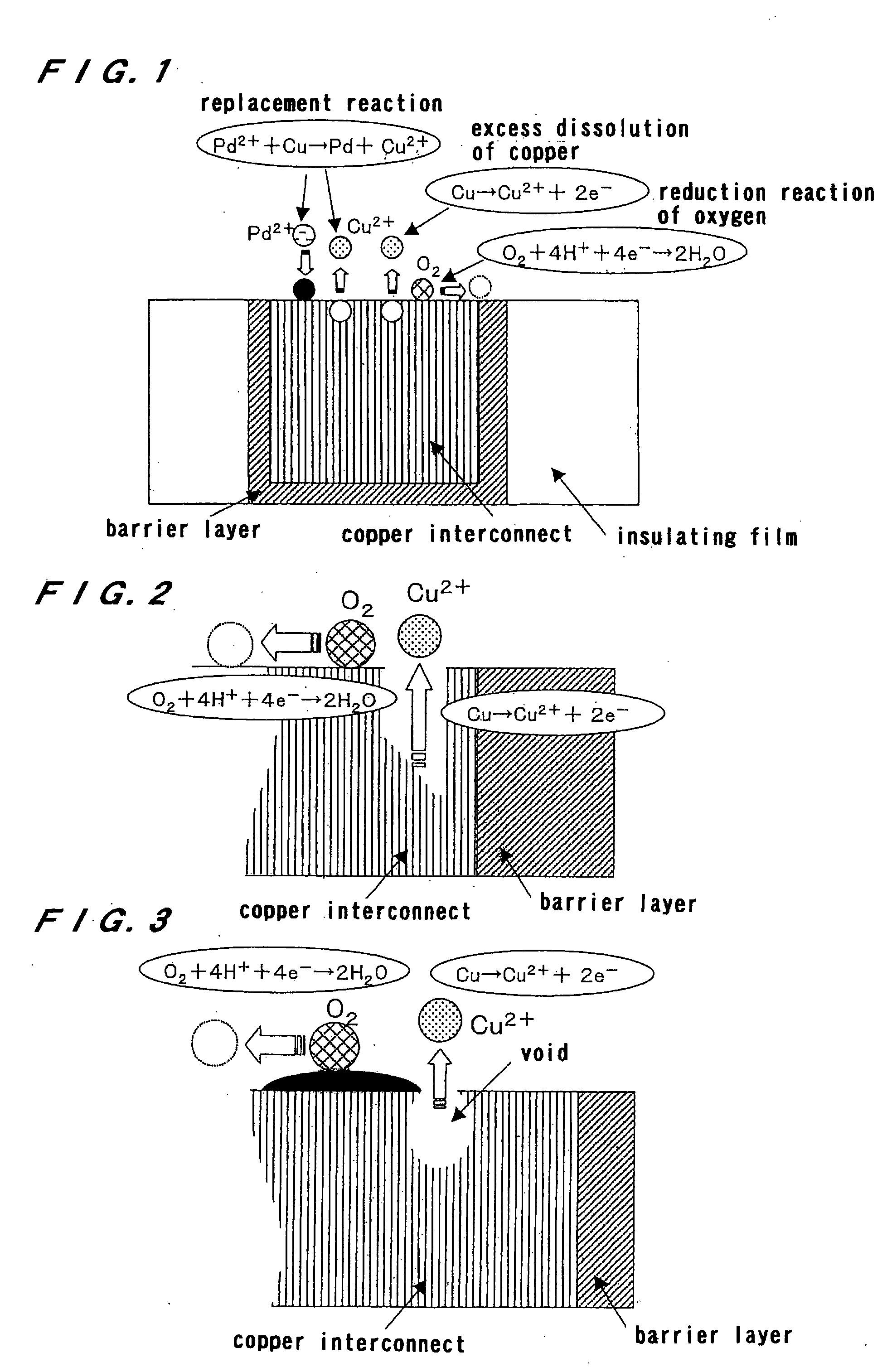
- Description
- Claims
- Application Information
AI Technical Summary
Benefits of technology
Problems solved by technology
Method used
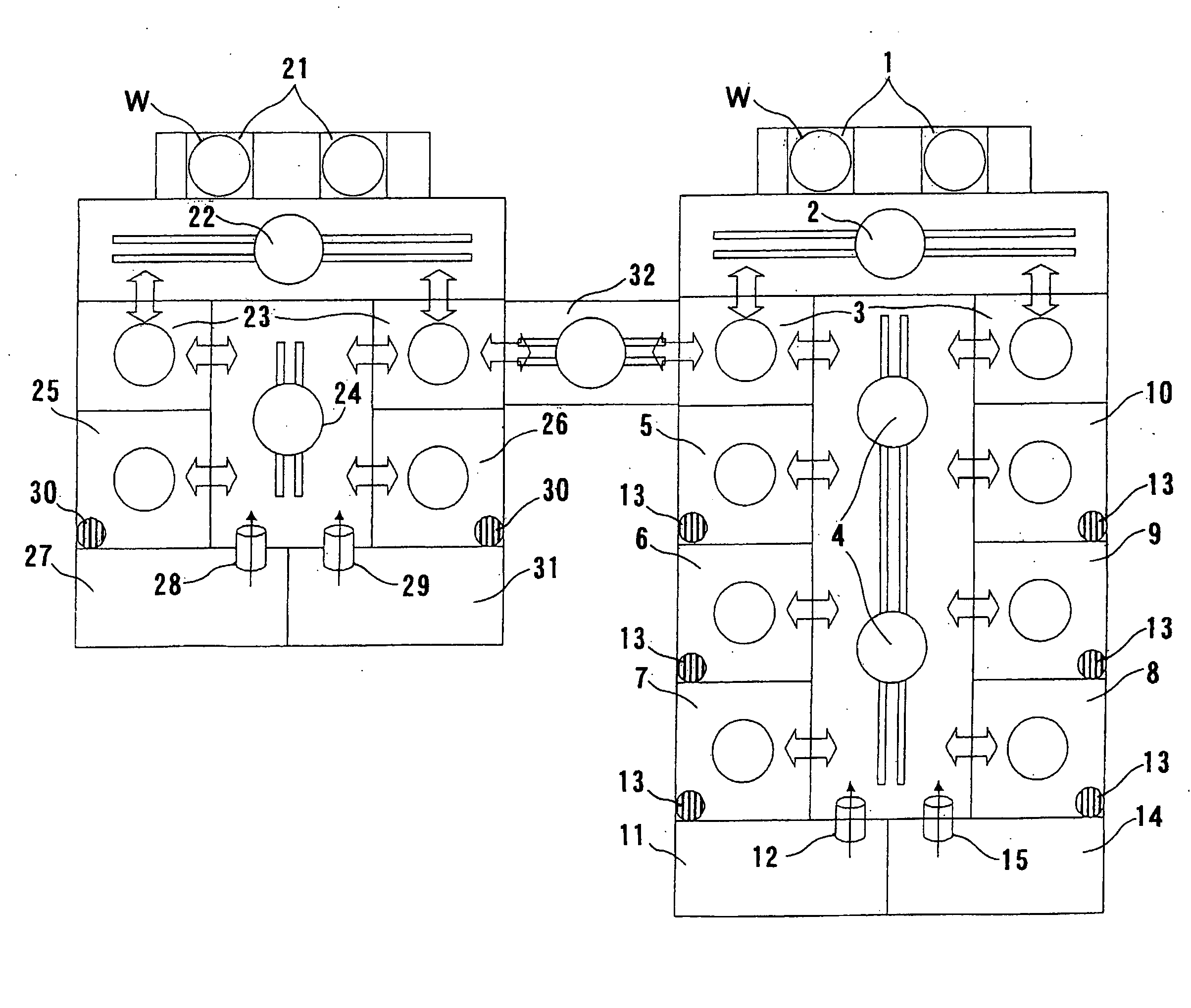
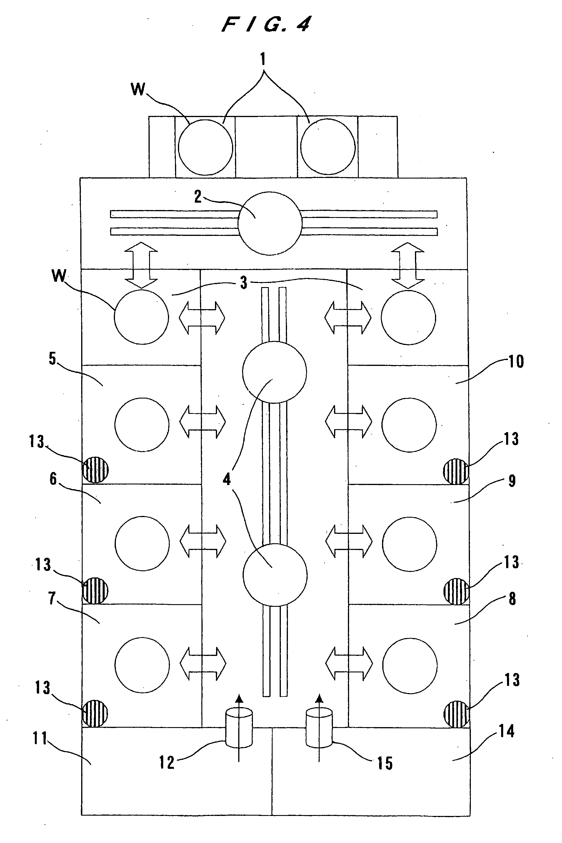
Image

Examples
example 1
[0115] Confirmation of variations of dissolution of copper in a case where deaeration is carried out or in a case where deaeration is not carried out:
[0116] The difference of variation of weight of copper was evaluated by using Electrochemical Quartz Crystal Microbalance in a case where a palladium sulfate solution was deaerated to create low oxygen concentration state and in a case where a palladium sulfate solution was not deaerated.
[0117] First, platinum was deposited on a crystal oscillator (manufactured by BAS Inc.) to produce a platinum electrode. Next, copper is deposited by a film thickness of about 0.1 μm on the platinum electrode using a plating solution used for formation of fine copper interconnects by electroplating.
[0118] On the other hand, a mixed liquid containing 50 mg / L of palladium sulfate and 50 g / L of sulfate was prepared as a catalyst-imparting solution. Then, the catalyst-imparting solution was deaerated to lower dissolved oxygen concentration to 1 ppm or l...
example 2
[0122] The relationship between dissolved oxygen concentration of a catalyst-imparting solution and interconnect resistance:
[0123] A catalyst-imparting solution containing 50 mg / L of palladium sulfate and 50 g / L of sulfate was prepared, and deaerated to various levels by bubbling nitrogen. According to the conventional method, electroplating was performed on the wafer, and then CMP was performed on the plated wafer to form copper interconnects. Then, catalyst was imparted to the copper interconnects using the catalyst-imparting solution, and then a cobalt tungsten phosphide (CoWP) film was formed by electroless plating under the following composition and conditions.
[0124] (CoWP Electroless Plating Solution)
composition:sodium hypophosphite10 g / Lcobalt sulfate 4 g / Lsodium citrate40 g / Lboric acid30 g / Lsodium tungstate 6 g / Lconditions:temperature of75° C.the solutionpH9(sodium hydroxide wasused for adjustmentof pH)agitationNo
[0125] The interconnect resistance of copper interconnects...
PUM
| Property | Measurement | Unit |
|---|---|---|
| Fraction | aaaaa | aaaaa |
| Concentration | aaaaa | aaaaa |
Abstract
Description
Claims
Application Information