Direct write process and apparatus

a technology of direct writing and process, which is applied in the direction of recording apparatus, manufacturing tools, instruments, etc., can solve the problems of insufficient application of large-scale rapid prototyping techniques, insufficient use of large-scale rapid prototyping methods, etc., to achieve rapid device prototyping and manufacturing, good combination of device accuracy and fabrication rate, and low-volume production run cost-effective

Active Publication Date: 2005-01-20
NANOTEK INSTR GRP LLC
View PDF7 Cites 165 Cited by
  • Summary
  • Abstract
  • Description
  • Claims
  • Application Information

AI Technical Summary

Benefits of technology

[0026] Good Combination of Device Accuracy and Fabrication Rate: By readily adjusting the pressure imposed on the fluid material, the droplet size and the droplet volume flow rate can be adjusted on demand at any time during the fabrication process. There is no need to change the dispensing head or the discharge orifice in order to vary the component accuracy or device-fabricating rate. This is in sharp contrast to most of the prior-art direct write methods in which component accuracy and fabrication rate are mutually exclusive.
[0027] Highly Versatile Process: The present invention provides a simple yet versatile process of rapid device prototyping and manufacturing. A user is free to choose the precursor fluid materials from a wide spectrum of material compositions. Further, two or three materials may be 26 combined to form a mixture, a composite, or a reaction product that constitutes a component with a desired combination of physical, chemical and electronic properties. There is essentially no constraint imposed on the kind of materials that can be fabricated into passive or active components of a microelectronic device.
[0028] Rapid Device Prototype Fabrication for Functional Testing: A prototype device may be designed and made to be similar or identical in both component compositions and geometric arrangement to the production device. Hence, the device prototype can be fully evaluated to verify the functional performance of a device before a photo-lithographic mask is fabricated (which is extremely expensive) or before mass production begins. This could help eliminate the possibility of producing an un-suitable mask or a large number of devices only to find out that these devices do not meet the functional requirements.
[0029] Cost-Effective Low-Volume Production Runs and Rapid Device Manufacturing: Rapid manufacturing of devices can be achieved in a more cost-effective fashion by using the presently invented proces

Problems solved by technology

Although DWM may also be accomplished in the sub-micron range using electron beams or focused ion beams, these techniques are not appropriate for large scale rapid prototyping due to their small scale and, hence, low deposition rates.
Due to the film material being vaporized by the action of the laser, LIFT is inherently a homogeneous, pyrolytic technique and typically cannot be used to deposit complex crystalline or multi-component materials.
Furthermore, because the material to be transferred is vaporized, it becomes more reactive and can more easily become degraded, oxidized or contaminated.
The method is not well suited for the transfer of organic materials, since many organic materials are fragile and thermally labile and can be irreversibly damaged during deposition.
Other shortcomings of the LIFT technique include poor uniformity, morphology, adhesion, and resolution.
Further, because of the high temperatures involved in the process, there is a danger of ablation or sputtering of the support, which can cause the incorporation of impurities in the material being deposited on the receiving substrate.
For some intended transfer materials, it may be difficult to find a suitable matrix material that is physically and chemically compatible with the transfer material so that the “lifting” procedure can be properly carried out.
Since a pulsed laser is also used in the MAPLE technique, this technique suffers from similar drawbacks that are commonly associated with the L

Method used


Image

  • Direct write process and apparatus
  • Direct write process and apparatus
  • Direct write process and apparatus

Examples


Embodiment Construction

[0038] Process and Apparatus:

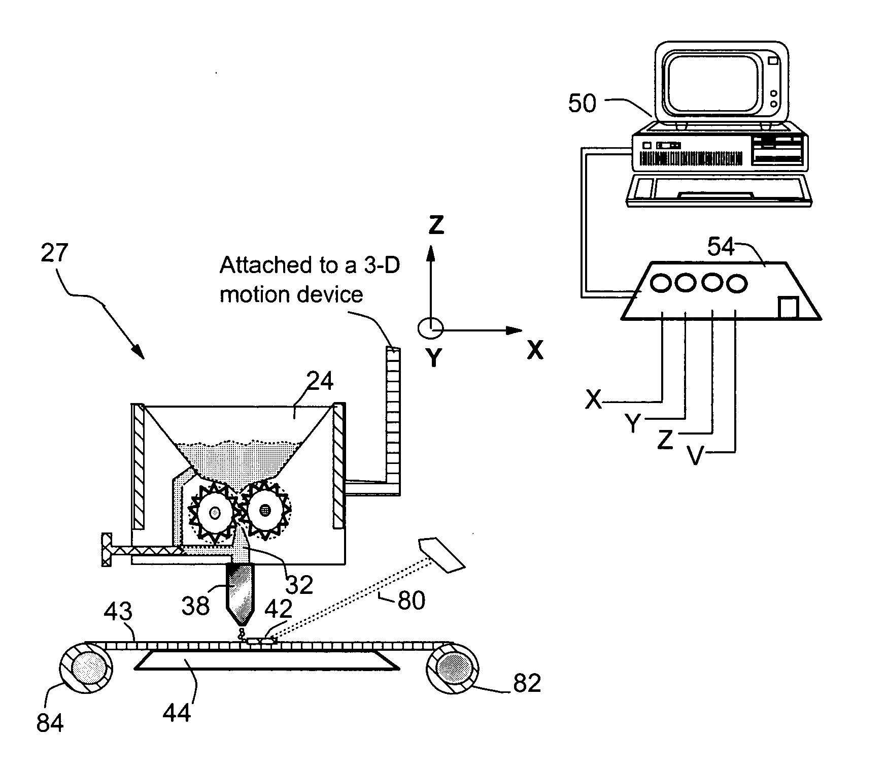
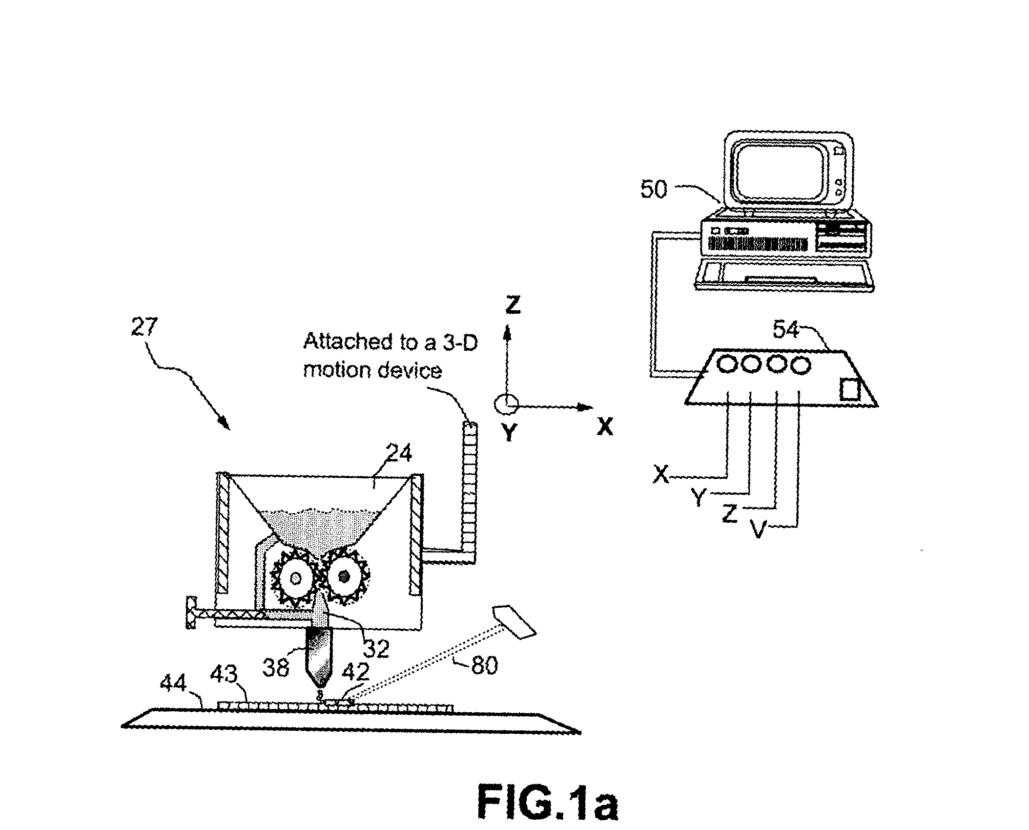
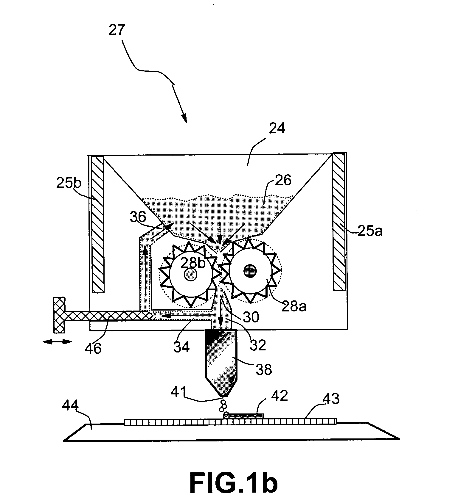
[0039]FIG. 1(a) illustrates one preferred embodiment of the presently invented process and apparatus for fabricating passive or active components onto a substrate surface to make a micro-electronic device, preferably on a point-by-point basis. The process begins with the creation of a computer-aided design (CAD in the form of a drawing, image, or geometry representation) of the device using a computer 50. This method further involves the operation of a system that includes computer software and control hardware, e.g., motion controller / indexer / servo 54. The system includes a support member 44 by which the device substrate 43 is supported while the device components are being deposited. The system also has an inkjet printhead-based dispensing head 38 for dispensing liquid droplets from a precursor fluid material 26. This material includes a liquid ingredient that helps to make the material in a flowable state while still residing in a chamber 32 of the d...


PUM

PropertyMeasurementUnit
Thicknessaaaaaaaaaa
Pressureaaaaaaaaaa
Flow rateaaaaaaaaaa

Abstract

A direct write process and apparatus for fabricating a desired circuit component onto a substrate surface of a microelectronic device according to a computer-aided design (CAD). The process includes (a) providing a support member by which the device is supported while being fabricated; (b) providing a chamber for containing a precursor fluid material under a substantially constant pressure differential relative to the ambient pressure, with the precursor fluid material having a viscosity no less than 10 cps; (c) operating an inkjet-based dispensing head with a control valve or actuator for dispensing and depositing minute droplets of the precursor fluid material onto the substrate surface; (d) energy- or heat-treat the deposited precursor fluid material for converting it to the desired active or passive component; and (e) operating a machine controller for generating control signals in response to the CAD coordinates for controlling the position of the dispensing head relative to the support member in response to the control signals to control dispensing and depositing of the precursor material to form the desired component. The process is useful for depositing a wide range of component materials onto an electronic device, including conductor, resistor, capacitor, dielectric, inductor, antenna, solar cell electrode, battery electrode, interconnect, superconductor, sensor, and actuator element materials.

Description

FIELD OF THE INVENTION [0001] This invention relates generally to a computer-controlled device-fabricating process and apparatus and, in particular, to an improved inkjet printing-based direct-write manufacturing process and apparatus for depositing desired active, passive, and other functional components to make an integrated circuit (IC) or a micro-electronic device such as a sensor, actuator, or micro-electro-mechanical system (MEMS). BACKGROUND OF THE INVENTION [0002] Direct write manufacturing (DWM) involves creating a pattern of active, passive and other functional components or elements directly onto a solid substrate, either by adding or removing material from the substrate, without utilizing a mask, pre-existing form, or tooling. DWM technologies were developed to answer the need of the microelectronics industry to have a means for rapidly prototyping circuit elements on various substrates. These elements are typically at the mesoscopic scale, i.e., within a size range betw...

Claims


Application Information

Patent Timeline
IPC IPC(8): B29C41/02B29C41/20B29C67/00G06F19/00
CPCB29C41/02B29C67/0059B29C41/20B29C64/112B33Y30/00B33Y10/00B33Y50/02
Inventor HUANG, WEN C.
Owner NANOTEK INSTR GRP LLC
Why Eureka
Try Eureka