Laser stimulated atom probe characterization of semiconductor and dielectric structures

Inactive Publication Date: 2005-01-27
CHISM II WILLIAM W
View PDF3 Cites 8 Cited by
  • Summary
  • Abstract
  • Description
  • Claims
  • Application Information

AI Technical Summary

Benefits of technology

The laser stimulated atom probe is capable of rapidly pulsing the ion emission current from a semiconductor or dielectric tip through the use of a pulsed ultraviolet (UV) laser. The optical absorption in semiconductor or dielectric materials is generally enhanced in the UV. This increased optical absorption provides efficient thermal pumping of the field evaporation rate. The enhanced optical absorption in the UV also allows the electric field at the tip to be reduced. Due to the enhanced absorption, a photo ionization mechanism may be realized, wherein the laser stimulates electronic transitions from the more extended surface atoms, thereby directly ionizing the surface atom. Additionally, the laser wavelength is selected nearby to strong optical absorption features such that the electric field at the tip may be used to further enhance the absorption through the Franz-Keldysh effect (Keldysh, 1958). This mechanism is available in all semiconductor and dielectric

Problems solved by technology

The main problem with conventional electrically pulsed atom probes is that they cannot be used to investigate samples with resistivity greater than approximately 10 Ohm-centimeter.
However, dielectrics and common semiconductors do not possess the conductivity required to support the short voltage pulsing needed to attain acceptable time of flight resolution, thus the atomic species cannot be resolved for dielectrics and common semiconductors using conventional voltage pulsed atom probes.
For this reason conventional voltage pulsed atom probes are limited to “high-conductivity” applications such as metals or low resistivity semiconductor materials.
Electrically pulsed atom probes also typically encounter difficulty in operation on samples of resistivity approximately 1 Ohm-centimeter or greater.
Thus, atom probe imaging of silicon samples with dopant levels below 5×10¹⁵ atoms per cubic centimeter (cm3) becomes difficult, and imaging of silicon samples with dopant levels below 5×10¹⁴ atoms per cm3 is impossible.
This “conductivity limit” is the principle impediment to the application of atom probe techniques to the dielectric and sem

Method used


Image

  • Laser stimulated atom probe characterization of semiconductor and dielectric structures
  • Laser stimulated atom probe characterization of semiconductor and dielectric structures
  • Laser stimulated atom probe characterization of semiconductor and dielectric structures

Examples


Embodiment Construction

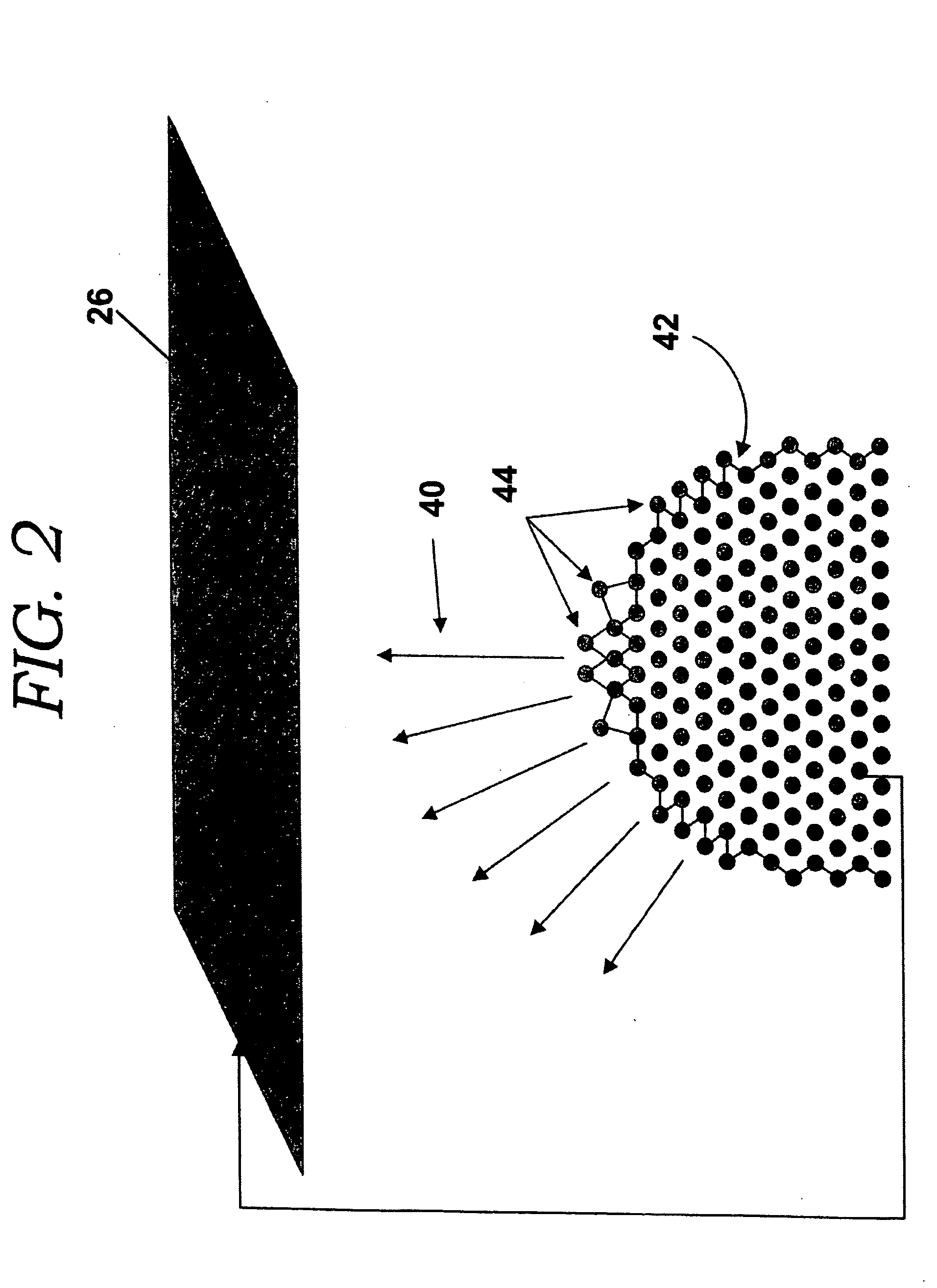
The following discusses use of the laser stimulated atom probe technique for atom probe microscopy of nanometer scale silicon tip structures. It is understood that the laser stimulated atom probe technique of the present drawings may be used to analyze any semiconductor or dielectric structure, the discussion of silicon structures considered to be exemplary only and in no way limiting in scope.

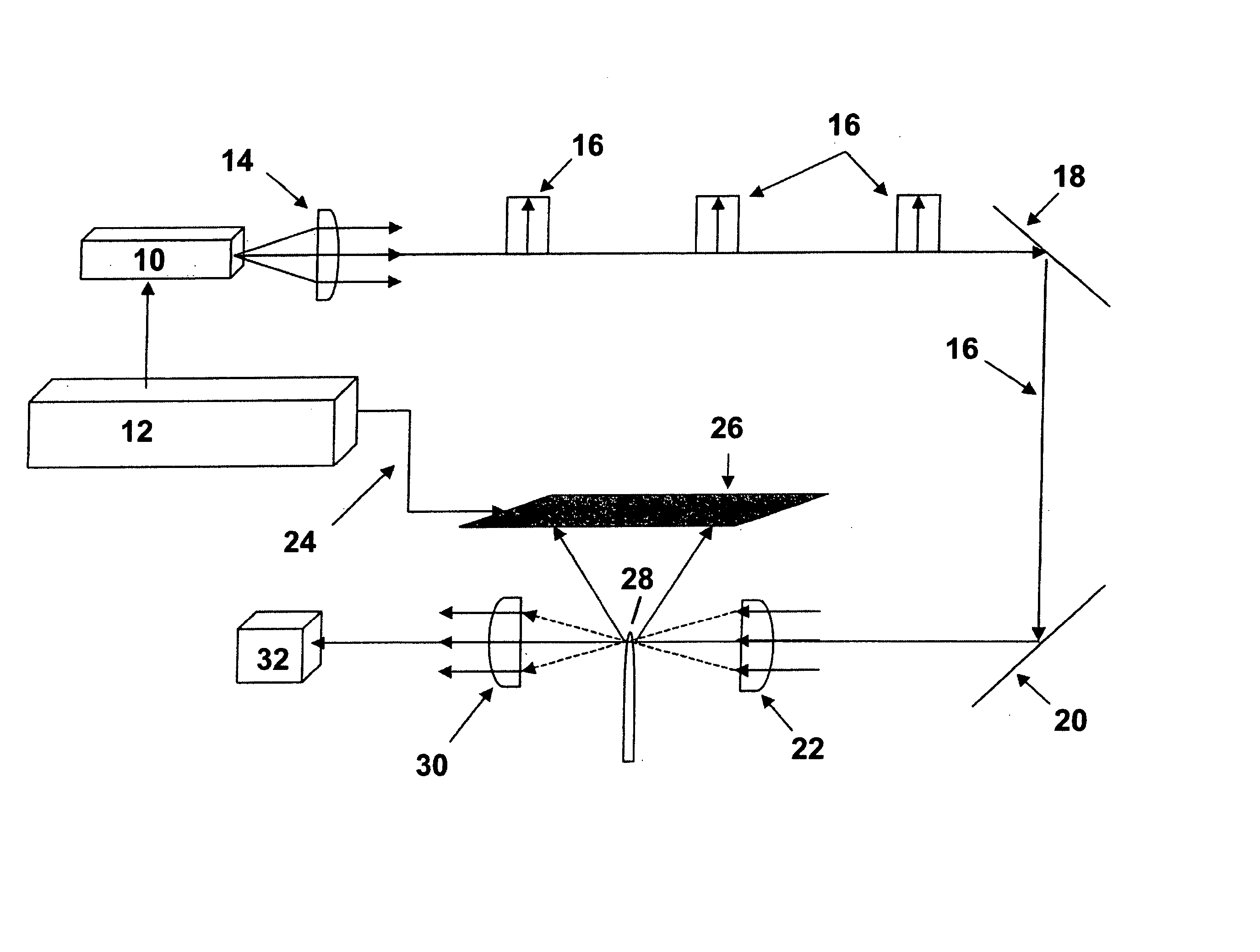
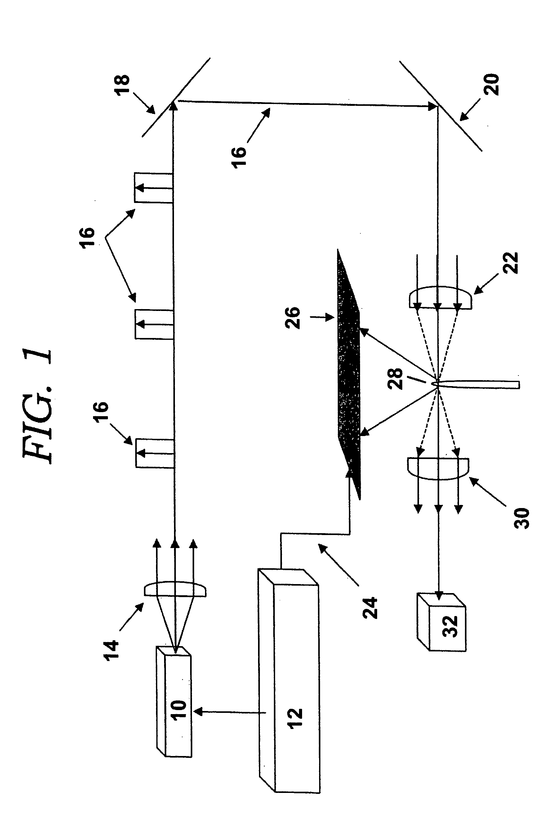
FIG. 1 illustrates a schematic arrangement of a laser stimulated atom probe, which utilizes a conventional atom probe providing a field emission tip and ion detector arrangement. The system shown in the drawing includes a laser 10 and laser controller 12. The laser controller directs the laser to produce short laser pulses and synchronous electronic timing signals 24 to the atom probe, which includes a position sensitive detector 26. Pulses of light 16 pass through an optical system that includes a collimation lens 14 mirrors 18, 20 and a microscope objective lens 22. The light is focused on...


PUM


Abstract

A laser stimulated atom probe for atom probe imaging of dielectric and low conductivity semiconductor materials is disclosed. The laser stimulated atom probe comprises a conventional atom probe providing a field emission tip and ion detector arrangement, a laser system providing a laser short laser pulse and synchronous electronic timing signal to the atom probe, and an optical system for delivery of the laser beam onto the field emitting tip apex. The conventional atom probe is employed in a manner similar to that used for investigation of high conductivity materials. However, the electric field is held static while the laser is pulsed to provide pulsing of the ion emission rate. The laser pulsing is accomplished in a manner similar to prior implementations of pulsed laser atom probe spectroscopy. The laser pulses provide a trigger signal to enable recording the time of flight in the atom probe. The laser operates at a wavelength in the UV in order to enhance the optical absorption in semiconductor or dielectric field emission tips. The increased optical absorption allows efficient thermal pumping of the field evaporation rate. The tip apex field is also used to redshift the optical absorption spectra of the dielectric or semiconducting material under investigation, further enhancing the optical absorption. Due to the enhanced absorption, it is also possible to realize a photo ionization mechanism, wherein the laser stimulates electronic transitions from the more extended surface atoms, thereby ionizing the surface atom. The laser source is collimated by a collimation lens, reflected using dielectric mirrors, directed onto the sample tip using a focusing lens arrangement, collected from the tip using a collection lens, and directed into a beam stop. The laser beam diameter at focus is approximately 3-30 microns, thus, individual emission tips may be scanned from a field of tips illuminated by the laser pulse.

Description

FIELD OF THE INVENTION The present disclosure relates generally to atom probe microscopy and more particularly to laser stimulated atom probe imaging of semiconductor and dielectric materials. BACKGROUND OF THE INVENTION Atom probe microscopes provide atomic scale structural resolution and species analysis of material surfaces. The atom probe consists of a field ion microscope used in conjunction with a time of flight mass spectrometer. Atom probes provide an atom by atom decomposition of a sharp sample “tip,” of approximately 100 nanometers in diameter. A positive voltage is applied across the sharp tip apex, to an electrode, resulting in a very strong electric field at the surface of the tip. Atoms at the surface of the tip become extended and evaporate from the surface through a physical process known as “field evaporation.” This process produces an ion near the tip which then travels toward the negative electrode. The onset of field evaporation occurs at electric fields on the...

Claims


Application Information

Patent Timeline
IPC IPC(8): G01Q70/00H01J37/285
CPCB82Y35/00G01Q70/00H01J37/285H01J2237/2855H01J49/161H01J2237/2852H01J49/0004
Inventor CHISM, WILLIAM W. II
Owner CHISM II WILLIAM W
Why Eureka
Try Eureka