Electroluminescence panel and manufacturing process therefor

a technology of electroluminescence panel and manufacturing process, which is applied in the manufacture of electrode systems, electric discharge tubes/lamps, and discharge tubes luminescent screens, etc., can solve the problems of reduced luminance, increased drive voltage, formation and growth of dark spots, etc., to improve the wettability of the substrate surface, reduce the generation of bubbles or microspaces, and eliminate microspaces quickly

Inactive Publication Date: 2005-02-03
SANYO ELECTRIC CO LTD
View PDF4 Cites 16 Cited by
  • Summary
  • Abstract
  • Description
  • Claims
  • Application Information

AI Technical Summary

Benefits of technology

[0018] Before the application step, the process can comprise the step of treating the surface of the first or the second substrate by ozone or plasma. Treatment by ozone or plasma can improve wettability of the substrate surface and lower a contact angle of the adhesive, so that the adhesive can be evenly extended on the substrate surface to give a smooth surface of the adhesive layer, which can prevent microspaces from being generated between the substrates during laminating them.
[0019] The lamination step can comprise the steps of placing the first and the second substrates in a vacuum apparatus, vacuuming the vacuum apparatus to a first pressure, increasing the pressure in the vacuum apparatus to a second pressure higher than the first pressure, and laminating the first and the second substrates under the second pressure. Before the step of vacuuming and after the step of increasing a pressure, the process may have the step of leaving the product for a given period for removing volatiles in the adhesive. It is preferable to laminating the substrates under a reduced pressure for preventing a bubble from remaining between the substrates. During the process, the volatiles in the adhesive may be released as bubbles. When the substrates are laminated during generation of bubbles, bubbles may remain between the substrates and irregularity may be formed on the adhesive surface, leading to formation of microspaces. Thus, after leaving the product under a reduced pressure for a given period for adequately removing the volatiles, a pressure is increased to a sufficient degree for inhibiting bubble generation before lamination. Thus, generation of bubbles or microspaces can be minimized.
[0020] The process may further comprise, after the lamination step, the step of heating the laminated substrates under an inert gas atmosphere or under a reduced pressure, or pressurizing the laminate under an inner pressure of the vacuuming apparatus higher than an ambient pressure. A gas which can be used for the inert gas atmosphere may be a rare gas such as argon or an unreactive gas such as nitrogen. The laminated substrates can be pressurized to rapidly eliminate microspaces remaining between the substrates which have been generated under a reduced pressure. During the pressurizing step, the laminate can be heated for reducing a viscosity of the adhesive to more effectively eliminate microspaces generated under a reduced pressure.
[0021] In the adhesive application step, different adhesives can be used for a first region comprising the electroluminescence element in the electroluminescence panel and a second region around the first region. An adhesive applied on the second region may be more moisture resistant or less water permeable than an adhesive applied on the first region. Thus, an inner EL element can be more effectively protected from moisture. The adhesive applied on the first region may be less shrinkable or more transparent than the adhesive applied on the second region. Thus, generation of a stress due to shrinkage of the adhesive can be prevented, resulting in improvement in display properties.

Problems solved by technology

An organic EL element is, however, extremely sensitive to moisture.
Specifically, an interface between a metal electrode and an organic layer may be deteriorated or broken due to moisture; a metal electrode may be oxidized, leading to a higher resistance; or an organic material itself may be degenerated due to moisture, resulting in problems such as increase in a drive voltage, formation and growth of dark spots and reduction in a luminance.
However, in these methods, a cover glass may be dislocated during the attachment step, or a cover glass may be deformed into a saddle shape.

Method used


Image

  • Electroluminescence panel and manufacturing process therefor
  • Electroluminescence panel and manufacturing process therefor
  • Electroluminescence panel and manufacturing process therefor

Examples


example 1

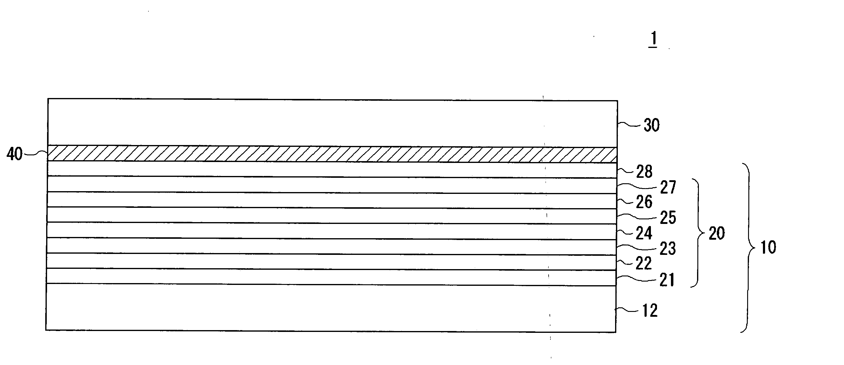
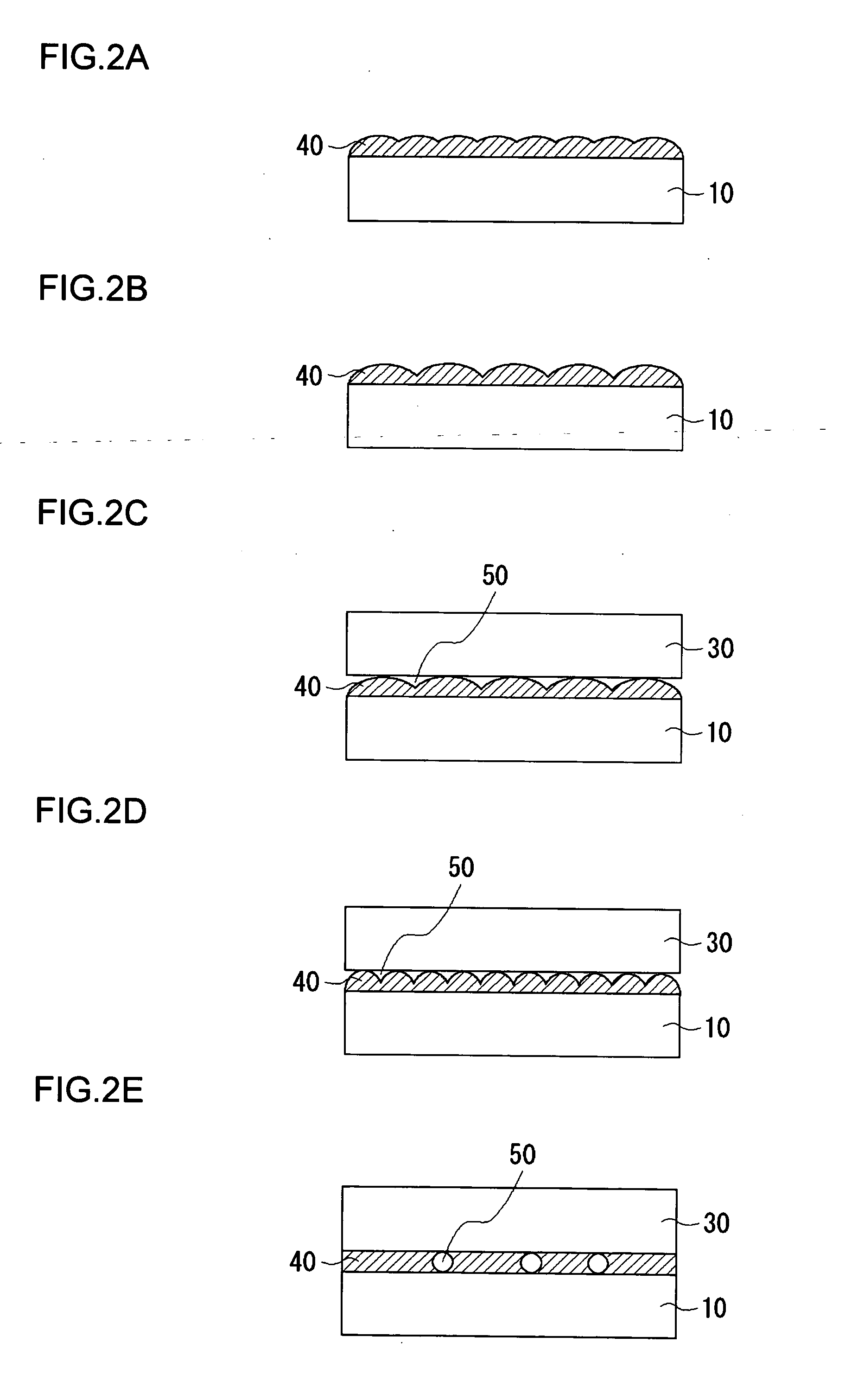
[0049] A protective film 28 consisting of an SiN inorganic layer was laminated on an organic EL element 20 deposited on a glass substrate 12, to prepare a device substrate 10. The device substrate 10 had a dimension of 2.2 inch (vertical)×2.2 inch (horizontal) and 220 (vertical)×176 (horizontal) pixels. Here, in a horizontal direction, three elements R, G and B are disposed per one pixel. In terms of a pixel size, a vertical longer side is 0.198 mm while a horizontal shorter side is 0.066 mm for each of R, G and B elements. The surface of the device substrate 10 was treated with plasma using argon. A contact angle was 10° or less. On the surface of the device substrate 10 was applied a UV curable epoxy resin with a viscosity of 2 Paxs by screen printing and the product was left for improving evenness. The device substrate 10 with the adhesive 40 was placed within a chamber in a vacuuming apparatus while a sealing substrate 30 without the adhesive 40 was placed on a substrate holder....

example 2

[0050] In this example, an organic EL panel 1 was manufactured as described in Example 1, except that both device substrate 10 and sealing substrate 30 were subjected to surface treatment. For the organic EL panel 1 manufactured in this example, the number of microspaces was 6 spaces with a diameter of 0.2 mm or less per a plane with 1 inch diagonal.

example 3

[0051] In this example, the procedure described in Example 1 was repeated except that in the lamination step substrates were laminated under a controlled pressure of P2 within the chamber as indicated as a solid line in FIG. 5 without surface treatment of the substrates. For the organic EL panel 1 manufactured in this example, the number of microspaces was 5 spaces with a diameter of 0.2 mm or less per a plane with 1 inch diagonal.


PUM


Abstract

A process for manufacturing a high quality organic EL panel is provided. On a glass substrate is formed an organic EL element, on which is then deposited a protective film. The surface of the device substrate or the sealing substrate is treated with ozone or plasma, and then an adhesive is applied on the surface by screen printing. After placing the device substrate and the sealing substrate in a chamber in a vacuuming apparatus, the inside of the chamber is vacuumed to a pressure of P1. After leaving the substrates for a given period until foaming of volatiles contained in the adhesive ceases, a pressure in the chamber is increased to P2 for preventing foaming of the volatiles, and then the substrates are laminated. Then, the laminate is pressurized and heated for removing microspaces. Finally, the adhesive is cured using, for example, a UV lamp.

Description

BACKGROUND OF THE INVENTION [0001] 1. Field of the Invention [0002] This invention relates to an electroluminescence panel; in particular, it relates to an electroluminescence panel having a structure where a sealing substrate is laminated on a substrate comprising an electroluminescence element and a manufacturing process therefor. [0003] 2. Description of the Related Art [0004] As information devices have been diversified, there has been increased the needs for a flat display device whose power consumption is smaller than a cathode ray tube (CRT) commonly used. As one of such flat display devices, an organic electroluminescence (hereinafter, referred to as “organic EL”) element has attracted attention, which exhibits good characteristics such as a higher efficiency, a thinner body, a light weight and less dependence on an angle of visibility. Thus, attempts have been made for developing a display utilizing such an organic EL element. [0005] Among various organic EL elements, an or...

Claims


Application Information

Patent Timeline
Patent Type & Authority Applications(United States)
IPC IPC(8): H01J1/62H05B33/10H01L51/50H01L51/52H05B33/04H05B33/14
CPCH01L51/5246H10K50/8426H05B33/10
Inventor HARADA, GAKUHAKU, HISAO
Owner SANYO ELECTRIC CO LTD
Why Eureka
Try Eureka