Selective etching of carbon-doped low-k dielectrics

Inactive Publication Date: 2005-02-03
APPLIED MATERIALS INC
View PDF28 Cites 280 Cited by
  • Summary
  • Abstract
  • Description
  • Claims
  • Application Information

AI Technical Summary

Benefits of technology

The present invention provides a process for etching a low-k dielectric layer with improved selectivity to adjacent layers and reduced microloading as compared to conventional low-k dielectric etching processes. In one embodiment of the present invention, the low-k dielectric layer is formed on a substrate with an underlying barrier/liner layer and an overlying photoresist mask. The substrate is placed in a plasm

Problems solved by technology

As the minimum feature size of integrated circuits continues to shrink, the metal lines become thinner and more densely packed, resulting in greater resistance in the metal lines and larger inter-metal capacitance, and therefore a longer time delay.
Among the many challenges presented by this process, etching trenches or vias in low-k dielectrics can be tricky due to the more complicated chemical composition of the dielectric material and the many differen

Method used


Image

  • Selective etching of carbon-doped low-k dielectrics
  • Selective etching of carbon-doped low-k dielectrics
  • Selective etching of carbon-doped low-k dielectrics

Examples


Embodiment Construction

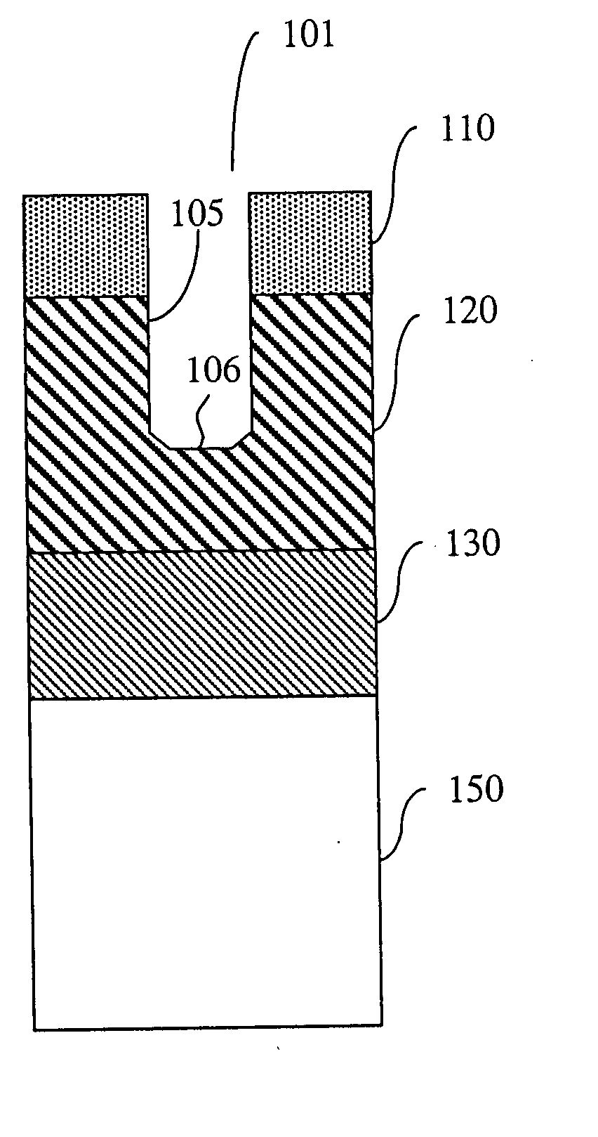
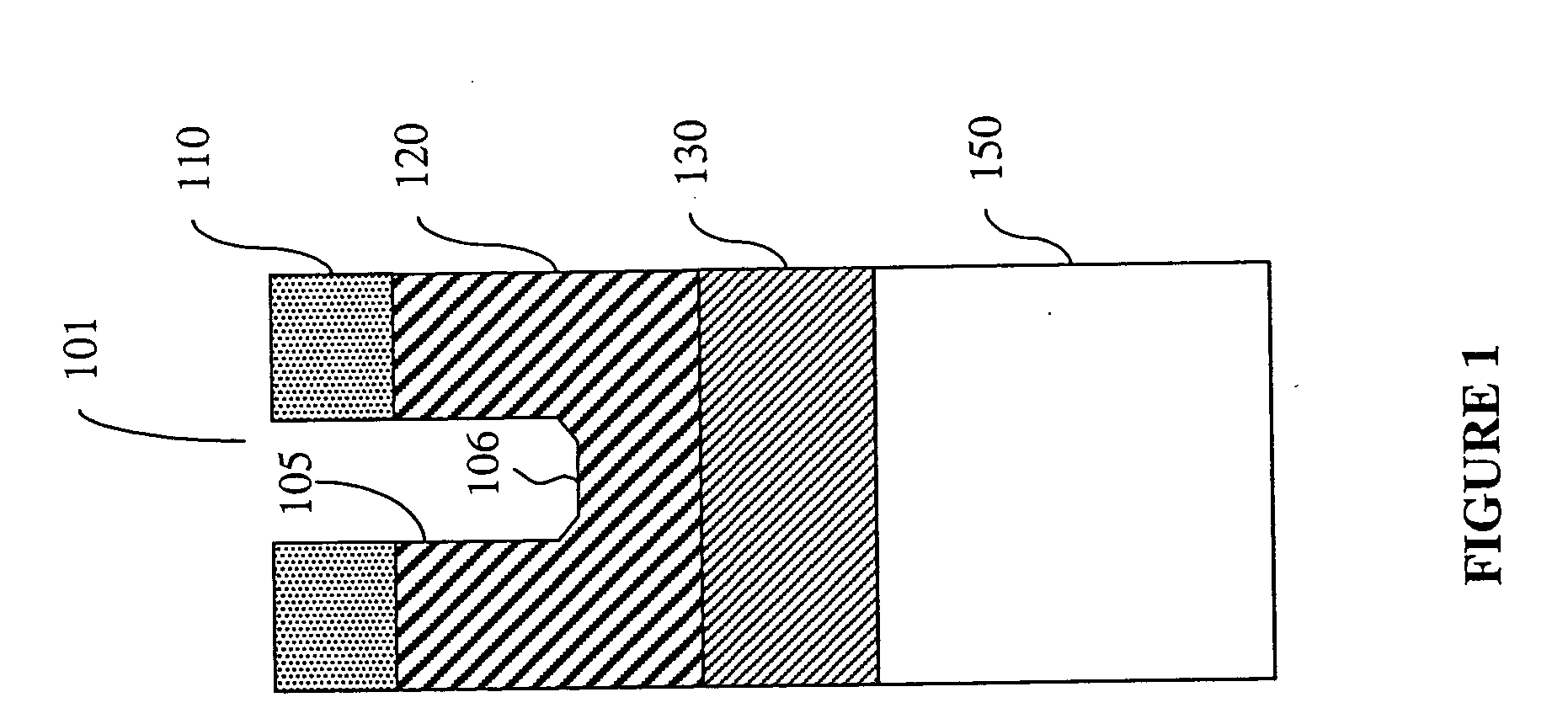
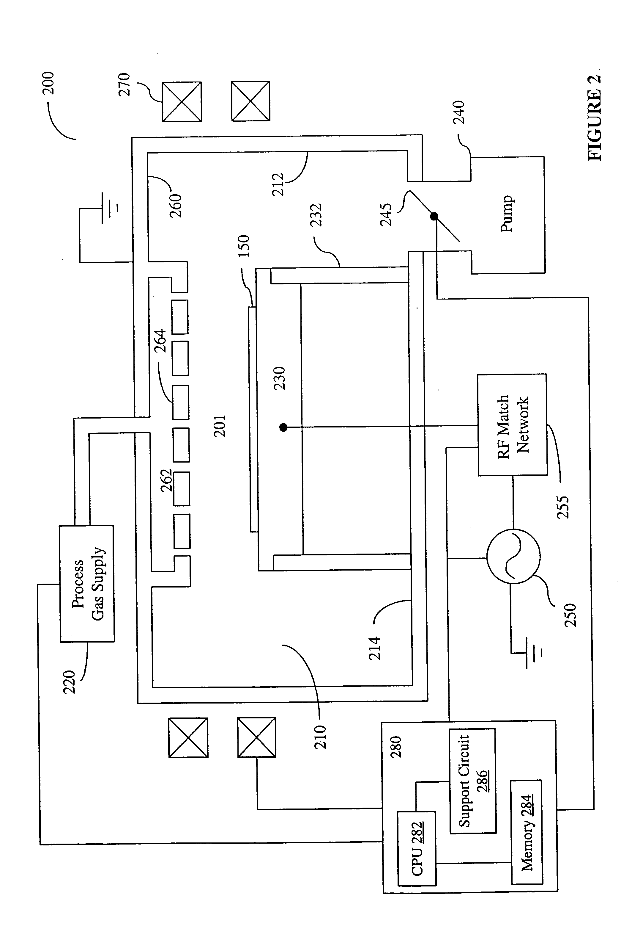
The following examples illustrate use of the present invention for etching the low-k dielectric layer 120 on substrate 150. An example of substrate 150 is a silicon wafer of 200 mm (8 inch) or 100 mm (12 inch) diameter. As shown in FIG. 1, the wafer 150 is coated successively with the barrier / liner layer 130 having a thickness of a few hundred angstroms, the low-k dielectric layer 120 having a thickness of about 0.4-1.5 micron, and a mask layer 110 of about 1930 Å that is patterned to define features such as feature 101 to be etched.

In the following examples, the mask layer is photoresist, such as “RISTON,” manufactured by duPont de Nemours Chemical Company. The low-k dielectric layer comprises carbon-doped dielectrics such as CH3 doped organo-silicate glass (OSG), organic polymers (e.g. benzocyclobutene, parylene, polytetrafluoroethylene, polyether, polyimide) or the like that are doped with a carbon-based dopant (e.g. CH3). The OSG is sometimes referred to as doped silicon diox...


PUM

PropertyMeasurementUnit
Fractionaaaaaaaaaa
Temperatureaaaaaaaaaa

Abstract

The present invention includes a process for selectively etching a low-k dielectric material formed on a substrate using a plasma of a gas mixture in a plasma etch chamber. The gas mixture comprises a fluorine-rich fluorocarbon or hydrofluorocarbon gas, a nitrogen-containing gas, and one or more additive gases, such as a hydrogen-rich hydrofluorocarbon gas, an inert gas and/or a carbon-oxygen gas. The process provides a low-k dielectric to a photoresist mask etching selectivity ratio greater than about 5:1, a low-k dielectric to a barrier/liner layer etching selectivity ratio greater about 10:1, and a low-k dielectric etch rate higher than about 4000 Å/min.

Description

The present application relates to semiconductor processing technologies, and particularly to etching patterns in a layer of dielectric material having low dielectric constant. BACKGROUND The maximum operating speed of current semiconductor devices is limited by the time delay factor T=RC of metal lines, where R is the resistance of the metal lines and C is the capacitance of the dielectric insulating material surrounding the metal lines. As the minimum feature size of integrated circuits continues to shrink, the metal lines become thinner and more densely packed, resulting in greater resistance in the metal lines and larger inter-metal capacitance, and therefore a longer time delay. By changing to different materials, i.e., higher conductivity material for the metal lines and lower permittivity (low-k) dielectric for the insulating material, device geometry can continue to shrink without adversely impacting the maximum operating speed. This has prompted the switch from aluminum a...

Claims


Application Information

Patent Timeline
IPC IPC(8): H01L21/3065H01L21/311
CPCY10S438/963H01L21/31116H01L21/3065
Inventor KIM, YUNSANGSHIN, NEUNGHOCHAE, HEEYEOPCHIU, JOEYYE, YANTIAN, FANGZHAO, XIAOYE
Owner APPLIED MATERIALS INC
Why Eureka
Try Eureka