Controlled sulfur species deposition process

a sulfur-bearing composition and control technology, applied in the direction of luminescent compositions, vacuum evaporation coatings, coatings, etc., can solve the problems that the phosphor composition may have a deleterious effect on the luminosity of the deposited phosphor composition, and achieve the effect of reducing the amount of sulfur-bearing species, preventing and/or minimizing the excess sulfur-bearing species, and ensuring the effect of reducing the amount o

Inactive Publication Date: 2005-02-24
IFIRE IP CORP
View PDF18 Cites 12 Cited by
  • Summary
  • Abstract
  • Description
  • Claims
  • Application Information

AI Technical Summary

Benefits of technology

[0005] The invention is a method for the deposition of multi element thin film compositions for thick film dielectric electroluminescent devices. In the method, the amount of sulfur is controlled in the deposition chamber during deposition of the thin film composition. In this manner, the amount of sulfur impinging on the deposition substrate, and thus incorporated into the thin film composition, is controlled. The method of the invention in particularly useful for the deposition of phosphor compositions comprising ternary, quaternary or higher sulfur-bearing compounds, preferably selected from the group consisting of thioaluminates, thiogallates and thioindates of at least one element from Groups IIA and IIB of the Periodic Table. Phosphors deposited in accordance with the method of the invention exhibit improved luminance and luminous efficiency compared with methods of the prior art.
[0006] In the method, one or more source materials that make up the composition of the deposited phosphor, are deposited onto a suitable substrate using for example, low pressure physical vapour deposition methods. The relative volatization of the source materials is controlled to obtain the desired ratio of metal species on the deposition substrate. A gettering or condensing material is provided substantially adjacent the source material(s) in order to remove, prevent and / or minimize any excess sulfur-bearing species from depositing on the deposition substrate and thus incorporating into the deposited phosphor composition. This is conducted at a temperature sufficiently low to prevent re-evaporation of the condensed sulfur-bearing species from the gettering or condensing material.
[0010] minimizing any excess quantity of sulfur-bearing species volatilized from the at least one source material from impinging on said substrate.
[0013] simultaneously minimizing any excess quantity of sulfur-bearing species volatilized from the at least one source material from impinging on said substrate; and
[0022] In a further embodiment of the invention, one or more agents may be further provided to: (a) minimize any excess of sulfur-bearing species that may also contain oxygen such as for example SO2; and, (b) to condense or remove molecular oxygen and / or water from the flux of evaporant emitted from the source material(s) and prevent it impinging on the deposition substrate within the deposition chamber. Oxygen may originate from the evaporation sources of sulfide if they contain one or more oxygen-bearing impurities such as sulfate or sulfite compounds and water. Such agents are preferably provided substantially adjacent the source material(s) used in the deposition method.

Problems solved by technology

An excess quantity of sulfur deposited within the phosphor composition may have a deleterious effect on the luminosity of the deposited phosphor composition.

Method used


Image

  • Controlled sulfur species deposition process
  • Controlled sulfur species deposition process
  • Controlled sulfur species deposition process

Examples


example 1

[0052] A thick film dielectric electroluminescent device was constructed incorporating thin film phosphor layers of barium thioaluminate activated with europium. The thick film substrate was a 5 cm by 5 cm alumina substrate having a thickness of 0.1 cm. Onto this substrate was deposited a gold electrode, followed with a thick film high dielectric constant dielectric layer in accordance with the methods exemplified in Applicant's co-pending international application PCT CA00 / 00561 filed May 12, 2000 (the disclosure of which is incorporated herein in its entirety). A 100-200 nm thin film dielectric layer of barium titanate was deposited on top of the thick film dielectric layer using the sol gel technique described in Applicant's co-pending U.S. patent application Ser. No. 09 / 761,971 filed Jan. 17, 2001 (the entirety of which is incorporated herein by reference).

[0053] A 600 nm thick barium magnesium thioaluminate phosphor film activated with about 3 atomic percent of europium with r...

example 2

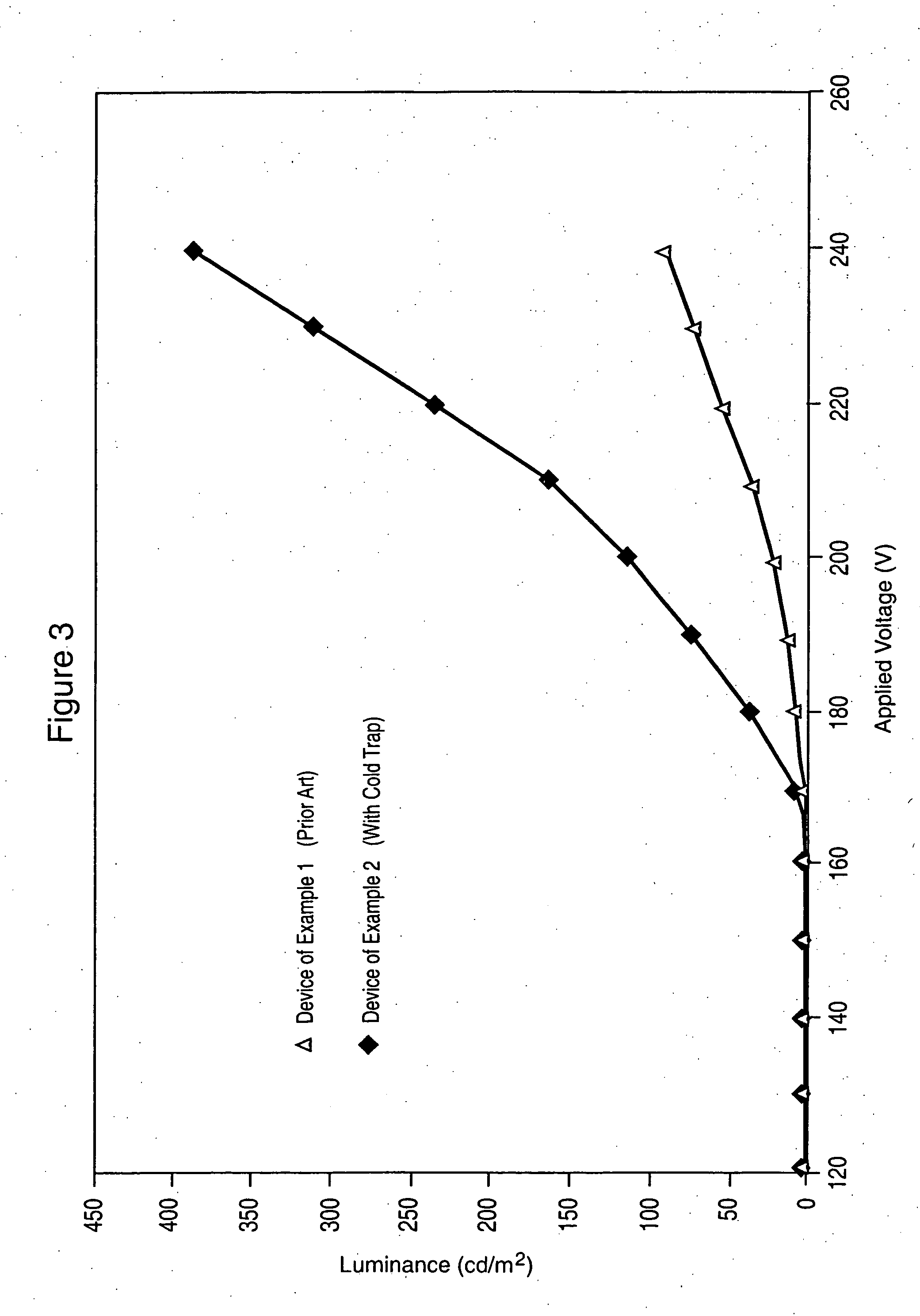
[0057] A device similar to that of example 1 was constructed but incorporating a cold trap adjacent to the barium sulfide source used for phosphor deposition. The cold trap was used to condense excess sulfur, oxygen and other volatile impurities. FIG. 3 shows the luminance as a function of applied voltage for this device. As can be seen from the data the luminance at 60 volts above the threshold voltage of 160 volts was about 240 candelas per square meter, more than three times that of the device of example 1.

[0058] A phosphor film deposited on a silicon wafer adjacent to the test sample was analyzed using XRD. It showed no sign of elemental sulfur. This example shows the benefits of the invention in preventing excess sulfur incorporation into the film and the attendant improvement realized in the device performance.

example 3

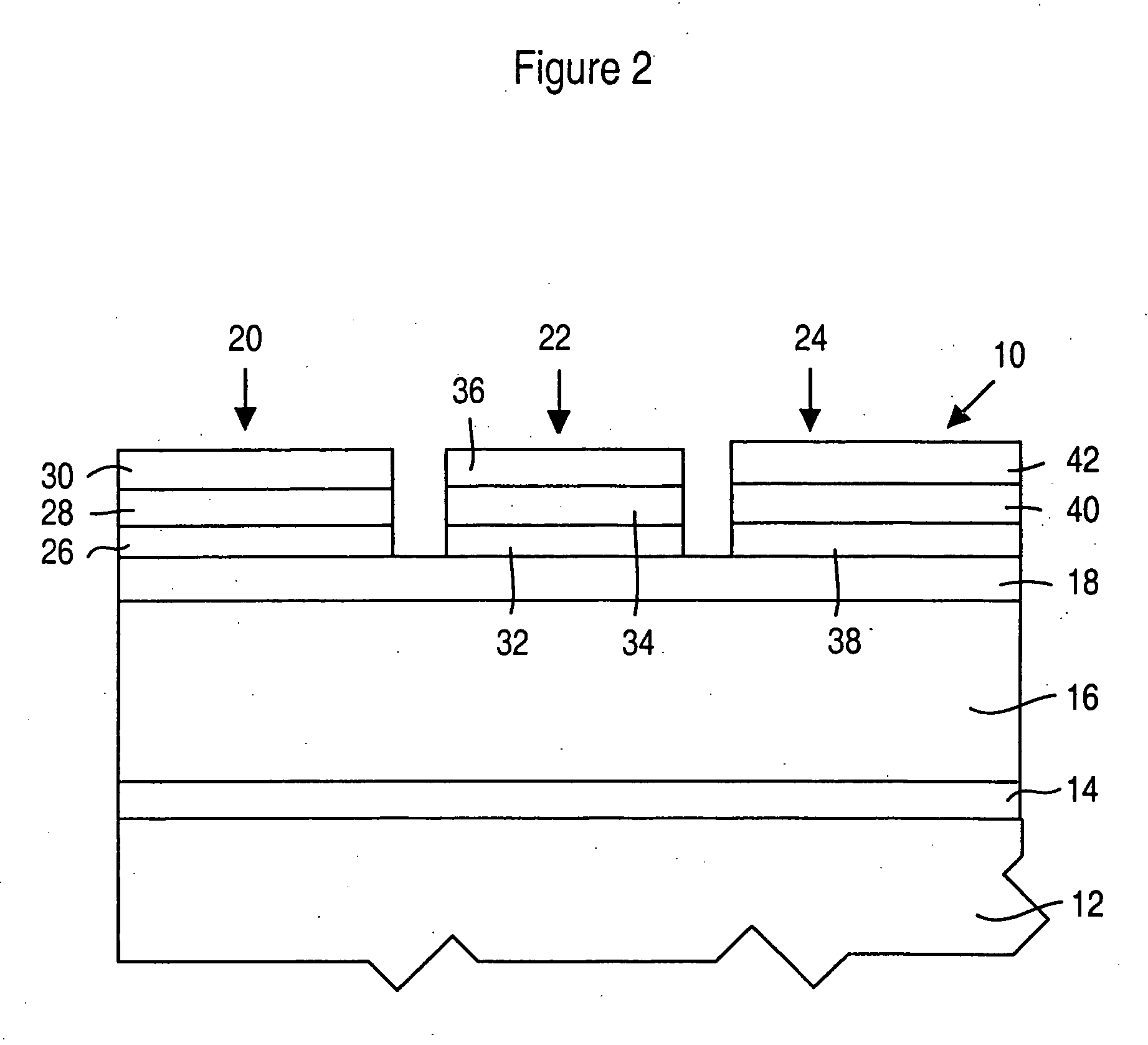
[0059] A thick film dielectric electroluminescent display of the type generally shown in FIG. 2 was fabricated. The thick film dielectric electroluminescent display was constructed on a 5 cm by 5 cm by 1.8 mm thick PD200 glass substrate obtained from Asahi Glass Co Ltd of Tokyo, Japan onto which was deposited a 200 nm thick barrier layer of aluminum nitride. A 0.8 μm thick gold electrode film was formed on the coated substrate by printing and firing a TR1207 gold-containing paste from Tanaka Kikinzoku International of Tokyo, Japan. Next, a composite thick film dielectric layer was fabricated on the gold lower electrode using the general methods described in Applicant's co-pending U.S. Patent Application 60 / 341,790 filed Dec. 21, 2002 (the entirety of which is incorporated herein by reference) but with specific process modifications described herein below.

[0060] The composite thick film dielectric layer was formed on the alumina coated glass using the following process. A thick film...


PUM

PropertyMeasurementUnit
temperatureaaaaaaaaaa
thicknessaaaaaaaaaa

Abstract

The present invention is a method for the deposition of a thin film of a pre-determined composition onto a substrate, the thin film comprising ternary, quaternary or higher sulfide compounds selected from the group consisting of thioaluminates, thiogallates and thioindates of at least one element from Groups IIA and IIB of the Periodic Table. The method comprises volatizing at least one source material of a sulfide of a pre-determined composition to form a sulfur-bearing thin film composition on a substrate and simultaneously inhibiting any excess quantity of sulfur-bearing species volatilized from the at least one source material from impinging on the substrate. The method improves the luminance and emission spectrum of phosphor materials used for full colour ac electroluminescent displays employing thick film dielectric layers with a high dielectric constant.

Description

FIELD OF THE INVENTION [0001] The present invention relates to a method for the deposition of multi element thin film compositions. More specifically, the invention is a method for the deposition of a phosphor composition where the amount of sulfur provided in the deposited phosphor composition is controlled. The method is particularly suitable for the deposition of phosphor compositions comprising a thioaluminate, thiogallate or thioaluminate of Group IIA and Group IIB elements where the source material(s) include sulfides that contain at least some of the elements comprising the deposited phosphor film. Further, the method is particularly useful for the deposition of phosphors for full colour ac electroluminescent displays employing thick film dielectric layers with a high dielectric constant. BACKGROUND TO THE INVENTION [0002] Thick film dielectric structures as exemplified by U.S. Pat. No. 5,432,015 (the entirety of which is incorporated herein by reference) are typically fabric...

Claims


Application Information

Patent Timeline
Patent Type & Authority Applications(United States)
IPC IPC(8): C09K11/77C09K11/84C23C14/00C23C14/06C23C14/54C23C16/06H05B33/10H05B33/14
CPCC09K11/7734C23C14/0021H05B33/14C23C14/548H05B33/10C23C14/0623C23C16/06C09K11/08C23C14/06C23C16/45525C23C14/34
Inventor XIN, YONGBAOSTILES, JIMLEUNG, CHI KITHUNT, TERRYACCHIONE, JOE
Owner IFIRE IP CORP
Why Eureka
Try Eureka