Unlock instant, AI-driven research and patent intelligence for your innovation.
Semiconductor device and a method of manufacturing the same
Active Publication Date: 2005-03-10
RENESAS ELECTRONICS CORP
View PDF8 Cites 22 Cited by
Summary
Abstract
Description
Claims
Application Information
AI Technical Summary
This helps you quickly interpret patents by identifying the three key elements:
Problems solved by technology
Method used
Benefits of technology
Benefits of technology
The present invention provides a semiconductor device for a mobile communication apparatus that uses a power MOSFET as an amplifying element. The invention aims to improve the power added efficiency of the amplifier circuit by reducing the on resistance and parasitic capacitance between the drain and gate, which are the main factors that affect power added efficiency. The invention proposes various techniques to achieve this, such as reducing the impurity concentration of the offset drain region and optimizing the layout of the source, drain, and gate. These techniques can lead to a reduction in chip size and lower power consumption of the mobile communication apparatus.
Problems solved by technology
Accordingly, one of the problems of a semiconductor device for a mobile communication apparatus which uses a power MOSFET as an amplifying element is to improve the power added efficiency of an amplifier circuit using a power MOSFET.
Another problem is to promote a size reduction of the chip on which a power MOSFET serving as an amplifying element is formed.
Method used
Image
Click on the blue label to locate the original text in one second.
Reading with bidirectional positioning of images and text.
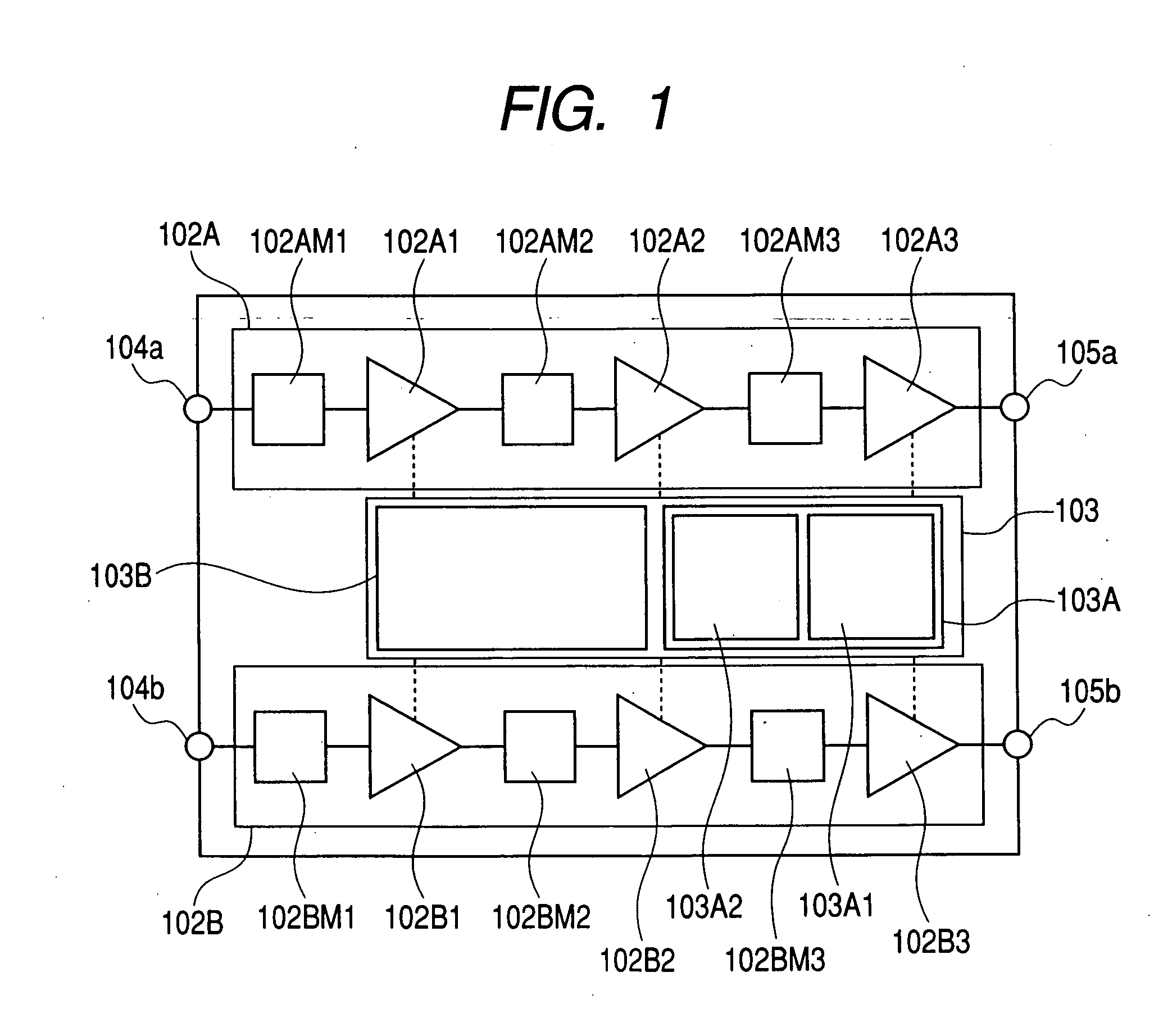
[0065]FIG. 1 is a block diagram of an amplifier circuit which constitutes the RF power module of Embodiment 1. In this diagram, there is illustrated an amplifier circuit to be used for an RF power module for which two frequency bands, for example, GSM900 and DCS1800, can be used (dual band system); and, at each frequency band, two communication systems, that is, a GMSK (Gaussian filtered Minimum Shift Keying) modulation system and an EDGE (Enhanced Data GSM Environment) modulation system, can be used.
[0066] The amplifier circuit has a power amplifier circuit 102A for GSM900, a power amplifier circuit 102B for DCS1800, and a peripheral circuit 103 which controls or assists the amplifying operation of each of the power amplifier circuits 102A and 102B. The powe...
embodiment 2
[0109] (Embodiment 2)
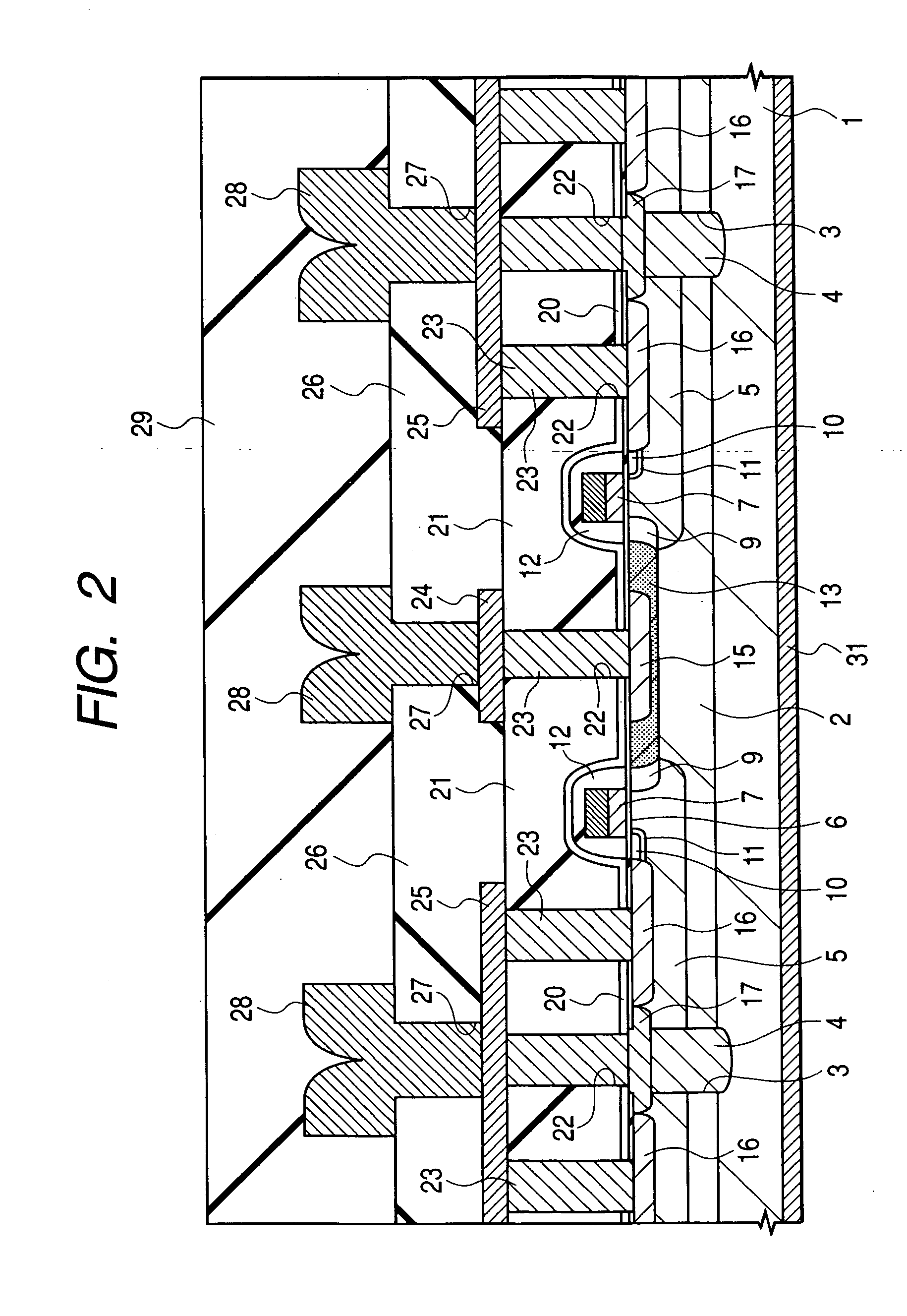
[0110] In the power MOSFET according to Embodiment 1, a p type sinker layer 4 is formed by embedding a heavily doped p type polysilicon film inside of the trench 3. The p type sinker layer 4 formed by the present method is advantageous over a sinker layer formed by ion implantation of an impurity, because the parasitic resistance of the former one can be made lower than that of the latter one.
[0111] However, formation of the sinker layer by embedding a conductive film inside of the trench requires the digging of a deep trench in the substrate 1 so that it imposes many restrictions on the process and disturbs free disposal of the sinker layer. More specifically, for the formation of a sinker layer by embedding a trench with a conductive film, such as polysilicon film or metal film, a trench with a high aspect ratio is dug first, and, then, a conductive film is filled in the trench without a space. The appearance of voids in the conductive film inside of the tren...
embodiment 3
[0119] (Embodiment 3)
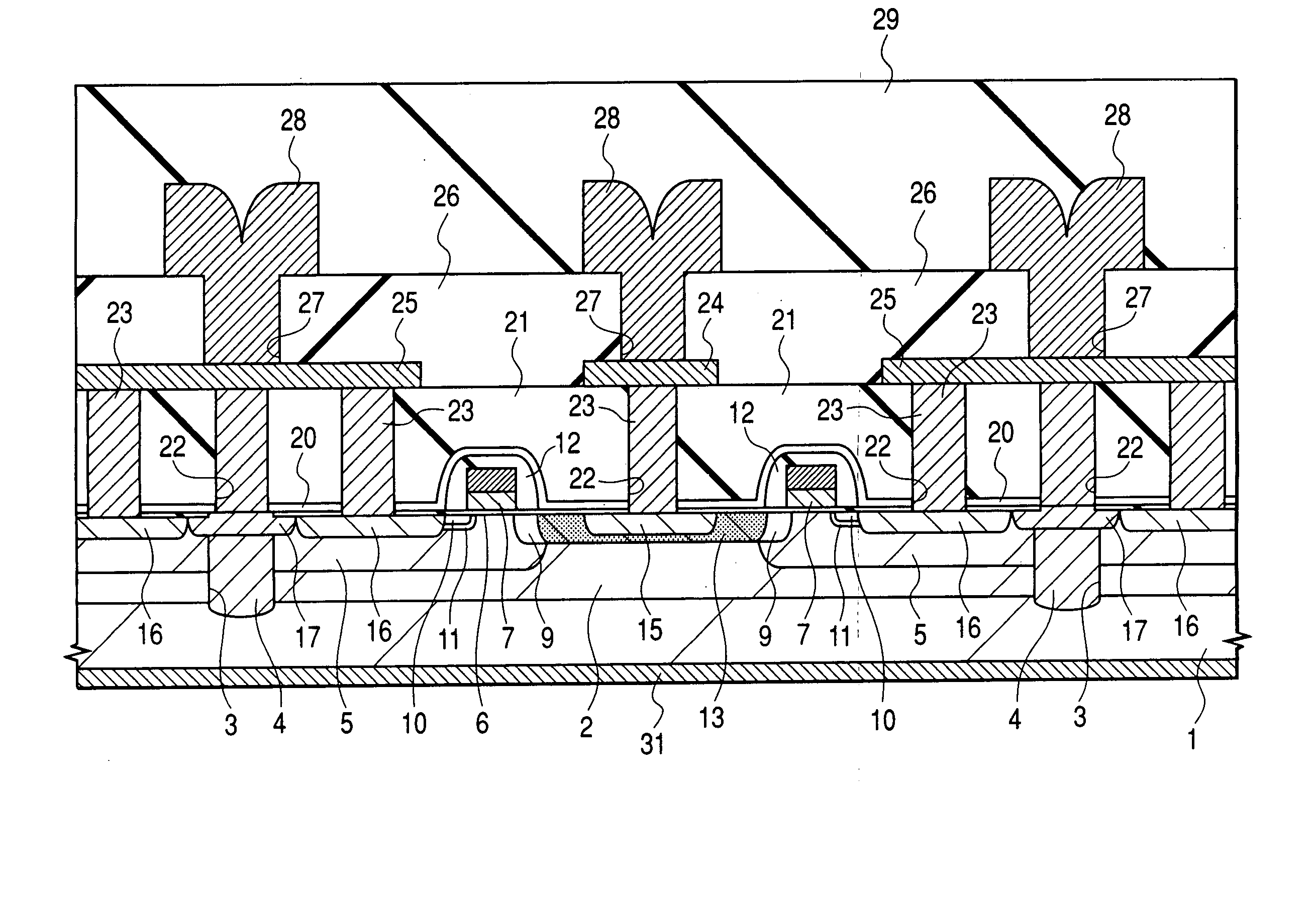
[0120]FIG. 27 is a fragmentary cross-sectional view of a substrate 1 illustrating a power MOSFET according to this Embodiment. In the n channel type power MOSFET of this Embodiment, a gate electrode 7 is composed only of an n type polysilicon film, a long trench 32 is formed in an insulating film over the gate electrode 7, and the gate electrode 7 is shunted by a plug 23 embedded inside of this long trench 32. The plug 23 is, similar to the plug 23 embedded inside of the contact hole 22, made of a metal film composed mainly of a W film. The long trench 32 has a length almost equal to that of the gate electrode 7 and extends in parallel to the gate electrode 7.
[0121] The long trench 32 over the gate electrode 7 is formed in the following manner. After deposition of a siliconoxide film 21 over the power MOSFET, the siliconoxide film 21 is dry etched using a photoresist film as a mask. Etching is once terminated on the surface of the silicon nitride film 21 cove...
PUM
Abstract
To reduce the size and improve the power added efficiency of an RF power module having an amplifier element composed of a siliconpower MOSFET, the on resistance and feedback capacitance, which were conventionally in a trade-off relationship, are reduced simultaneously by forming the structure of an offset drain region existing between a gate electrode and an n+ type drain region of the power MOSFET into a double offset one. More specifically, this is accomplished by adjusting the impurity concentration of an n− type offset drain region, which is closest to the gate electrode, to be relatively low and adjusting the impurity concentration of an n type offset drain region, which is distant from the gate electrode, to be relatively high.
Description
CROSS-REFERENCE TO RELATED APPLICATION [0001] The present application claims priority from Japanese Patent application JP2003-313971, filed on Sep. 5, 2003, the content of which is hereby incorporated by reference into this application. BACKGROUND OF THE INVENTION [0002] The present invention relates to a semiconductor device to be used for mobile communication apparatuses (so called mobile phones) and to a technique for the manufacture thereof, particularly to a technique that is effective when applied to a semiconductor device to be mounted on an RF (Radio Frequency) power module. [0003] In recent years, mobile communication apparatuses (so called mobile phones), which employ a communication system typified by GSM (Global System for Mobile Communications), PCS (Personal Communication Systems), PDC (Personal Digital Cellular) system or CDMA (Code Division Multiple Access) system, have gained widespread use throughout the world. [0004] In general, such mobile communication apparatus...
Claims
Application Information
Patent Timeline
Application Date:The date an application was filed.
Publication Date:The date a patent or application was officially published.
First Publication Date:The earliest publication date of a patent with the same application number.
Issue Date:Publication date of the patent grant document.
PCT Entry Date:The Entry date of PCT National Phase.
Estimated Expiry Date:The statutory expiry date of a patent right according to the Patent Law, and it is the longest term of protection that the patent right can achieve without the termination of the patent right due to other reasons(Term extension factor has been taken into account ).
Invalid Date:Actual expiry date is based on effective date or publication date of legal transaction data of invalid patent.
Patent Type & Authority Applications(United States)

