

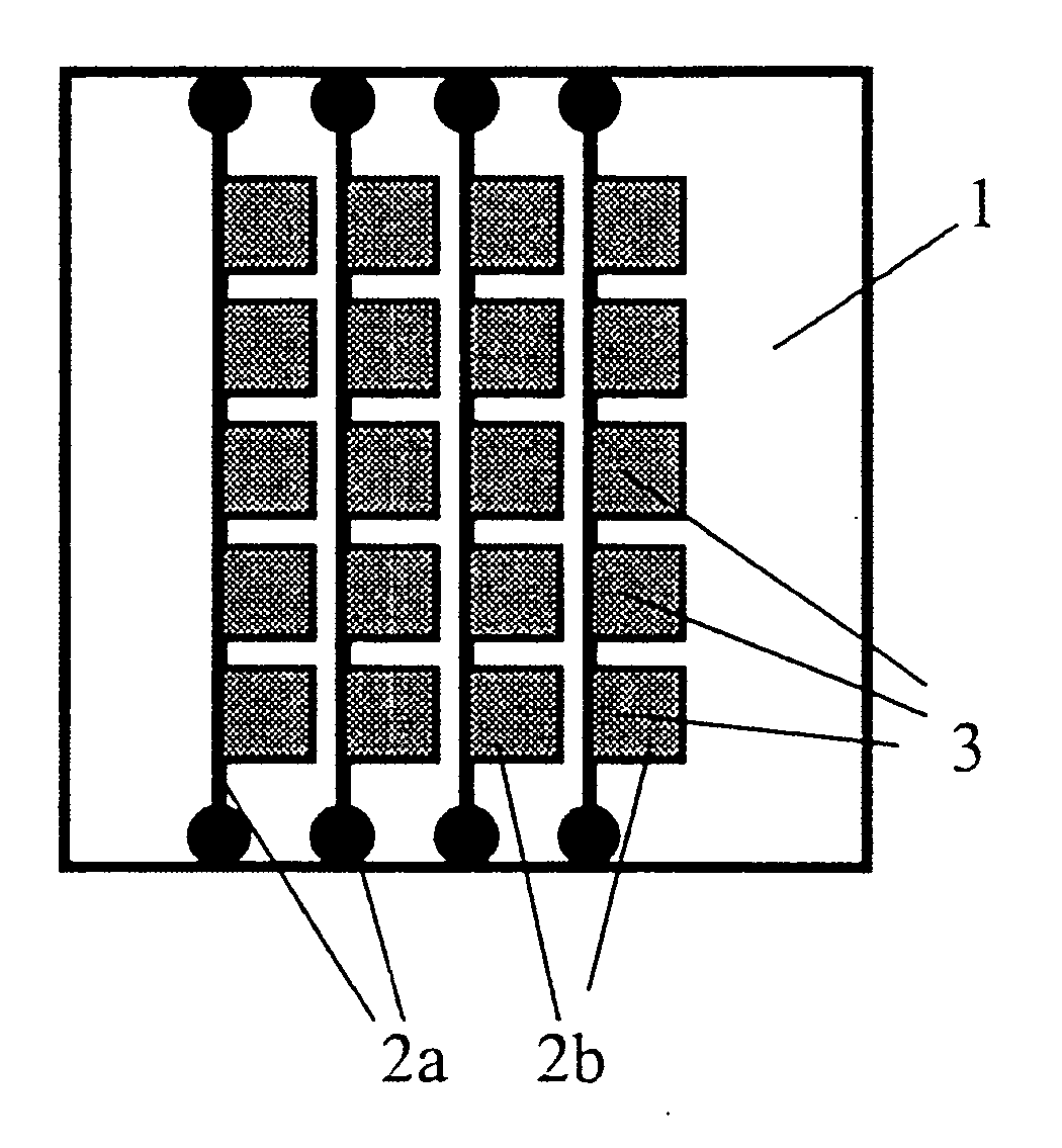
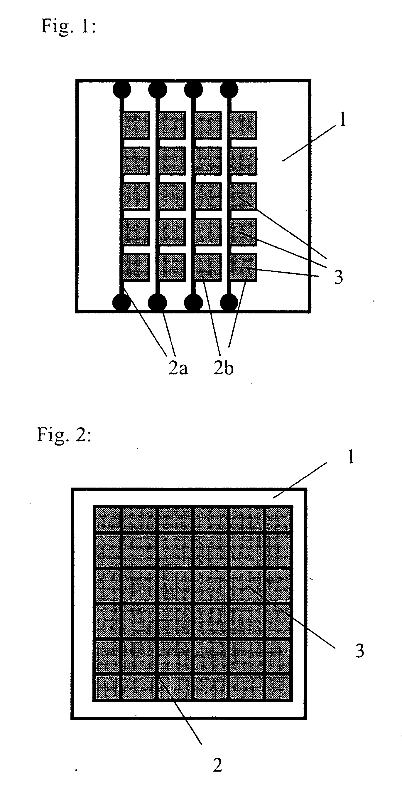
Transparent electrode for electro-optical structures
a technology of transparent electrodes and electro-optical structures, applied in the direction of conductive layers on insulating supports, non-metal conductors, natural mineral layered products, etc., can solve the problems of complex and expensive, difficult to achieve, and difficult to construct very thin lighting elements
- Summary
- Abstract
- Description
- Claims
- Application Information
AI Technical Summary
Benefits of technology
Problems solved by technology
Method used
Image

Examples
example 1
1. Structured Substrates
ITO-coated glass substrates (Merck Display) are cut to a size of 50×50 mm2 and cleaned. The ITO coating is then coated with photopositive resist (available from JSR, LCPR 1400G-80cP) and this is exposed through a printed polymer film (shadow mask) after drying. The shadow mask comprises isolated transparent circles that are 5 mm in diameter and are arranged in a square at intervals of 10 mm. After exposure and drying, the uncrosslinked photoresist is removed from the circle regions with the developer solution (available from JSR, TMA238WA). At these points, which are now unmasked, the ITO is subsequently removed with an etching solution consisting of 47.5% by volume distilled water, 47.5% by volume hydrochloric acid (32%), 5.0% by volume nitric acid (65%), the crosslinked photo resist is then removed with acetone and the structured ITO substrate is finally cleaned.
2. Production of the In Situ PEDT Layers:
Epoxysilane (Silquest® A187, OSi specialities) i...
example 2
Method as in Example 1 but Omitting Step 3 (Application of the PEDT:PSS Layer).
Summary of Results of Examples 1 and 2:
CurrentdensityVoltageLuminanceEfficiencyOLED structure[mA / cm2][V][cd / m2][cd / A]ITO / / in situ PEDT / / 1025.11050.10PEDT:PSS / / MEH-PPV / / Ca / / Ag(cf. Example 1)in situ PEDT / / 1026.01020.10PEDT:PSS / / MEH-PPV / / Ca / / Ag(cf. Example 1)ITO / / in situ PEDT / / 1026.6190.019MEH-PPV / / Ca / / Ag(cf. Example 2)in situ PEDT / / MEH-1026.3160.016PPV / / Ca / / Ag(cf. Example 2)
This shows that the luminance and efficiency of OLEDs with a luminescent area of at least 0.049 cm2 are not dependent on whether or not the ITO is located below the in situ PEDT layer. Comparison of Examples 1 and 2 also shows that a PEDT:PSS layer between the in situ layer and the MEH-PPV layer (emitter layer) significantly improves the luminance.
example 3
Method as in Example 1 with the Following Difference in Step 4 (Application of the Emitter Layer):
5 mL of a 0.25% by weight chloroform solution of PF-F8 (Poly(9,9-dioctyl-fluorene)), a blue emitter synthesised by Yamamoto's method of polymerisation, which is described in detail in the literature, for example, T. Yamamoto et al., J. Am. Chem. Soc. 1996, 118, 10389-10399, and T. Yamamoto et al., Macromolecules 1992, 25, 1214-1223) are filtered (Millipore HV, 0.45 μm) and distributed on the dried PEDT:PSS layer. The supernatant solution is then spun off by rotating the plate for 30 seconds at 200 rpm. The substrate coated in this way is then dried on a heating plate for 5 min at 110° C. The total layer thickness is 130 nm.
PUM
| Property | Measurement | Unit |
|---|---|---|
| Dispersion potential | aaaaa | aaaaa |
| Transmission | aaaaa | aaaaa |
| Electrical conductor | aaaaa | aaaaa |
Abstract
Description
Claims
Application Information