Amplifier and frequency converter

Inactive Publication Date: 2005-03-24
PANASONIC CORP
View PDF9 Cites 26 Cited by
  • Summary
  • Abstract
  • Description
  • Claims
  • Application Information

AI Technical Summary

Benefits of technology

[0016] Therefore, an object of the present invention is to provide a negative feedback amplifier and a negative feedback frequency converter each of simple structure, capable of providing negative feedback of the phases of a fundamental wave and a third-order intermodulation wave of an input signal to the input, and suitable for integration into a semiconduct

Problems solved by technology

However, insertion of the resistance at the input side causes severe degradation in noise characteristics.
Insertion of the resistance at the output side, on the other hand, causes severe degradation in distortion characteristics.
However, the above first through sixth conventional examples have a drawback that due to only one type of shunt feedback path being provided for each conventional example, the feedback circuit is complex in structure and large in size in order to shift the feedback signal in phase by approximately 180 degrees with respect to the input signal.
Therefore, thi

Method used


Image

  • Amplifier and frequency converter
  • Amplifier and frequency converter
  • Amplifier and frequency converter

Examples


first embodiment

[0049] (First Embodiment)

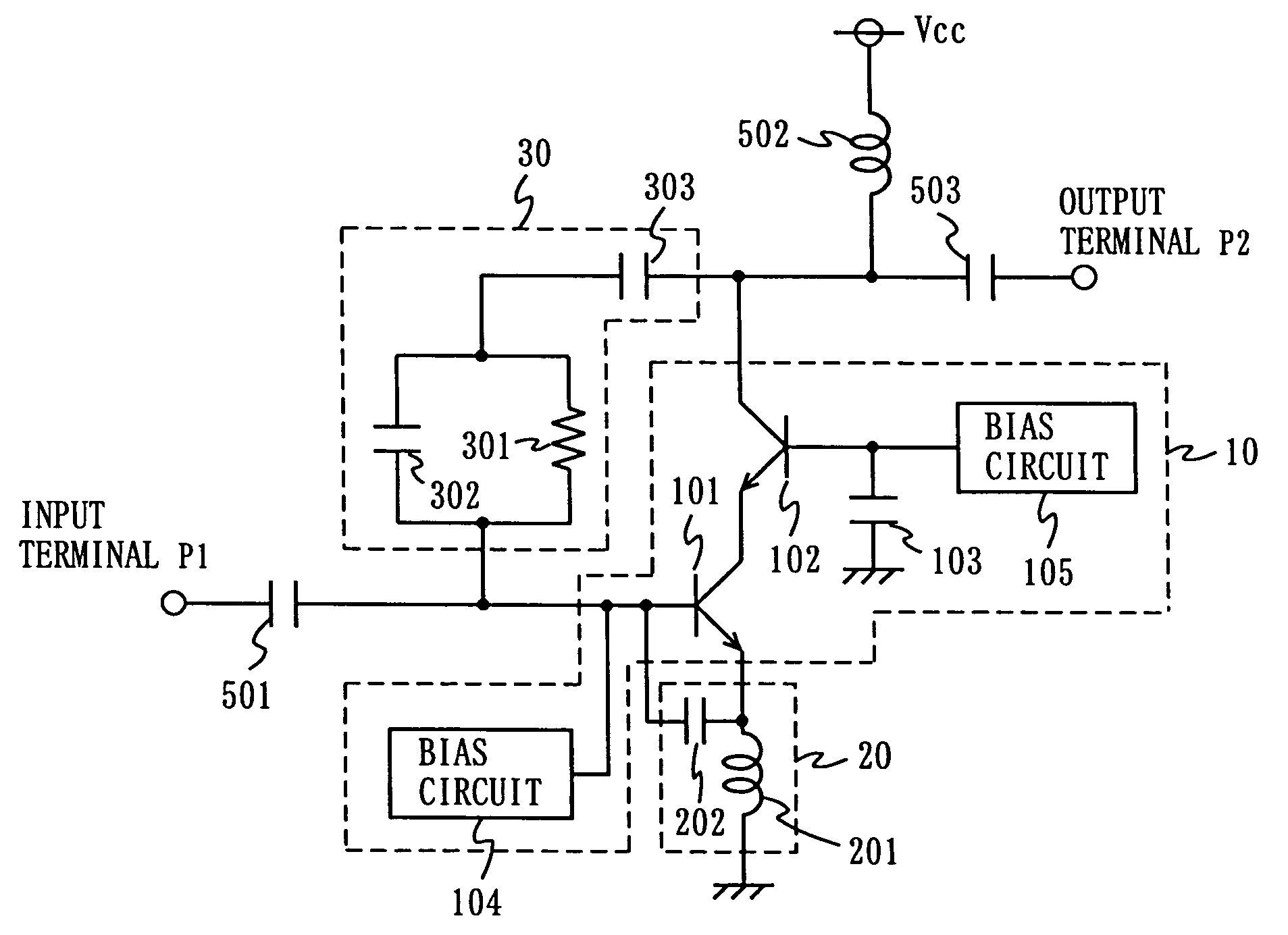
[0050]FIG. 1 is a circuit diagram of an amplifier according to a first embodiment of the present invention. The amplifier as shown in FIG. 1 includes an amplifier circuit 10, a first feedback circuit 20, a second feedback circuit 30, a DC cut capacitors 501 and 503, and a choke inductor 502. This amplifier has a feature where the operations of the first feedback circuit 20 and the second feedback circuit 30 cause a phase of a signal in which fundamental waves included in two feedback signals are combined and a phase of a signal in which second harmonics included in two feedback signals are combined to be shifted by approximately 180 degrees from a phase of a fundamental wave of an input signal. Also, the amplifier is used mainly in a high frequency band.

[0051] The amplifier circuit 10 includes bipolar transistors 101 and 102, a bypass capacitor 103, and bias circuits 104 and 105. The amplifier circuit 10 amplifies a signal inputted from an input terminal P1...

second embodiment

[0061] (Second Embodiment)

[0062]FIG. 3 is a circuit diagram of an amplifier according to a second embodiment of the present invention. The amplifier as illustrated in FIG. 3 differs from that according to the first embodiment in that it is structured by a differential pair. The operation and effect of the amplifier which will be described below are similar to those of the amplifier according to the first embodiment, and therefore descriptions thereof are omitted. Hereinafter, only the circuit configuration will be described.

[0063] The amplifier as illustrated in FIG. 3 includes an amplifier circuit 15, a first feedback circuit 25, a second feedback circuit 35, DC cut capacitors 501a, 501b, 503a, and 503b, and choke inductors 502a and 502b. The amplifier circuit 15, the first feedback circuit 25, and the second feedback circuit 35 are exemplary modifications of the amplifier circuit 10, the first feedback circuit 20, and the second feedback circuit 30 according to the first embodime...

third embodiment

[0067] (Third Embodiment)

[0068]FIG. 4 is a circuit diagram of an amplifier according to a third embodiment of the present invention. The amplifier as illustrated in FIG. 4 is similar to that according to the second embodiment, except that the first feedback circuit 25 is replaced by a first feedback circuit 26. Therefore, in FIG. 4, components similar to those according to the second embodiment are provided with the same reference numerals, and are not described herein.

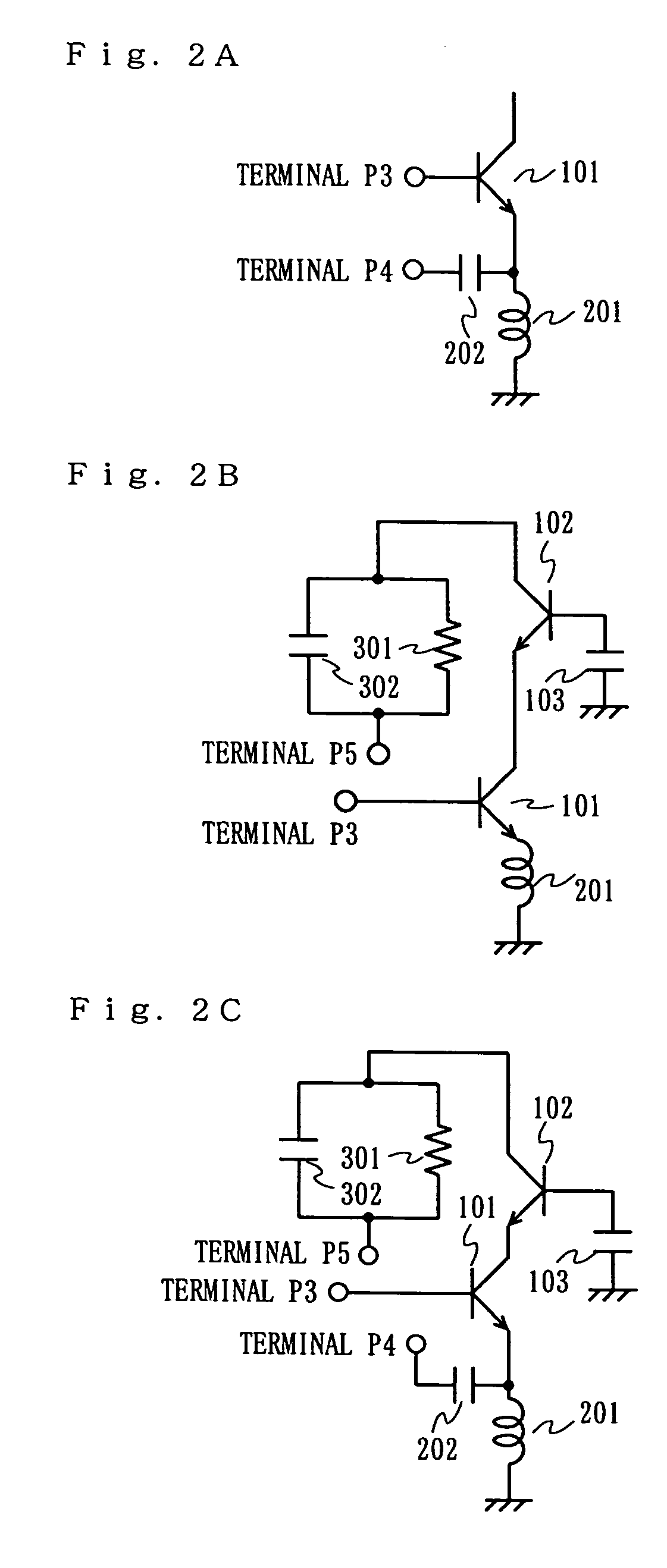
[0069] The first feedback circuit 26 includes inductors 201a, 201b, and 203, and capacitors 202a and 202b. As with the second embodiment, the emitters of the bipolar transistors 101a and 101b are connected to the inductors 201a and 201b, respectively, at one end each. At the other end each, the inductors 201a and 201b are connected to each other, and their connecting point Q2 is grounded via the inductor 203. The capacitor 202a is inserted between the emitter and base of the bipolar transistor 101a, whereas the capac...


PUM


Abstract

An amplifier circuit 10 amplifies a signal inputted from an input terminal P1. A first feedback circuit 20 is placed across an emitter of a bipolar transistor 101 and an input of the amplifier circuit 10. A second feedback circuit 30 is placed across the input and an output of the amplifier circuit 10 for feeding the output of the amplifier circuit 10 back to the input. A phase change amount in the feedback circuit is determined by the values of an inductor and a capacitor. The values of these elements are selected so that a phase of a signal in which fundamental waves included in two feedback signals are combined and a phase of a signal in which second harmonics included in the two feedback signals are combined are shifted by approximately 180 degrees from a phase of a fundamental wave of an input signal.

Description

BACKGROUND OF THE INVENTION [0001] 1. Field of the Invention [0002] The present invention relates to amplifiers for amplifying an input signal, and frequency converters for amplifying an input signal and then converting the frequency of the amplified signal. More specifically, the present invention relates to an amplifier and a frequency converter both having a wide dynamic range and suitable for integration into a semiconductor integrated circuit. [0003] 2. Description of the Background Art [0004] In receivers of a wireless system, typified by cellular phones, a signal received at an antenna is amplified by an amplifier circuit at an initial stage. Such an initial-stage amplifier circuit is required to have characteristics of achieving low noise and high gain when receiving a weak signal, while achieving low distortion and low gain when receiving a large signal. Particularly, in recent mobile communications, since the characteristics of a reception electric field are greatly varied...

Claims


Application Information

Patent Timeline
IPC IPC(8): H03F1/22H03F1/34H03F3/19H03F3/45
CPCH03F1/22H03F1/34H03F3/19H03F3/45089H03F2203/45464H03F2200/372H03F2200/492H03F2203/45256H03F2200/144
Inventor NAKATANI, TOSHIFUMIITOH, JYUNJINAKANO, HIDEO
Owner PANASONIC CORP
Why Eureka
Try Eureka