
Method for forming nanoscale features and structures produced thereby

a technology of features and structures, applied in the field of nanoscale features and structures produced by thereby, can solve the problems of negligible energy delivered and insignificant radiation damage beyond the optical breakdown region, and achieve the effect of reducing the size of features and significant impact in biological sciences

Inactive Publication Date: 2005-03-24
RGT UNIV OF MICHIGAN
View PDF20 Cites 49 Cited by
  • Summary
  • Abstract
  • Description
  • Claims
  • Application Information

AI Technical Summary

Benefits of technology

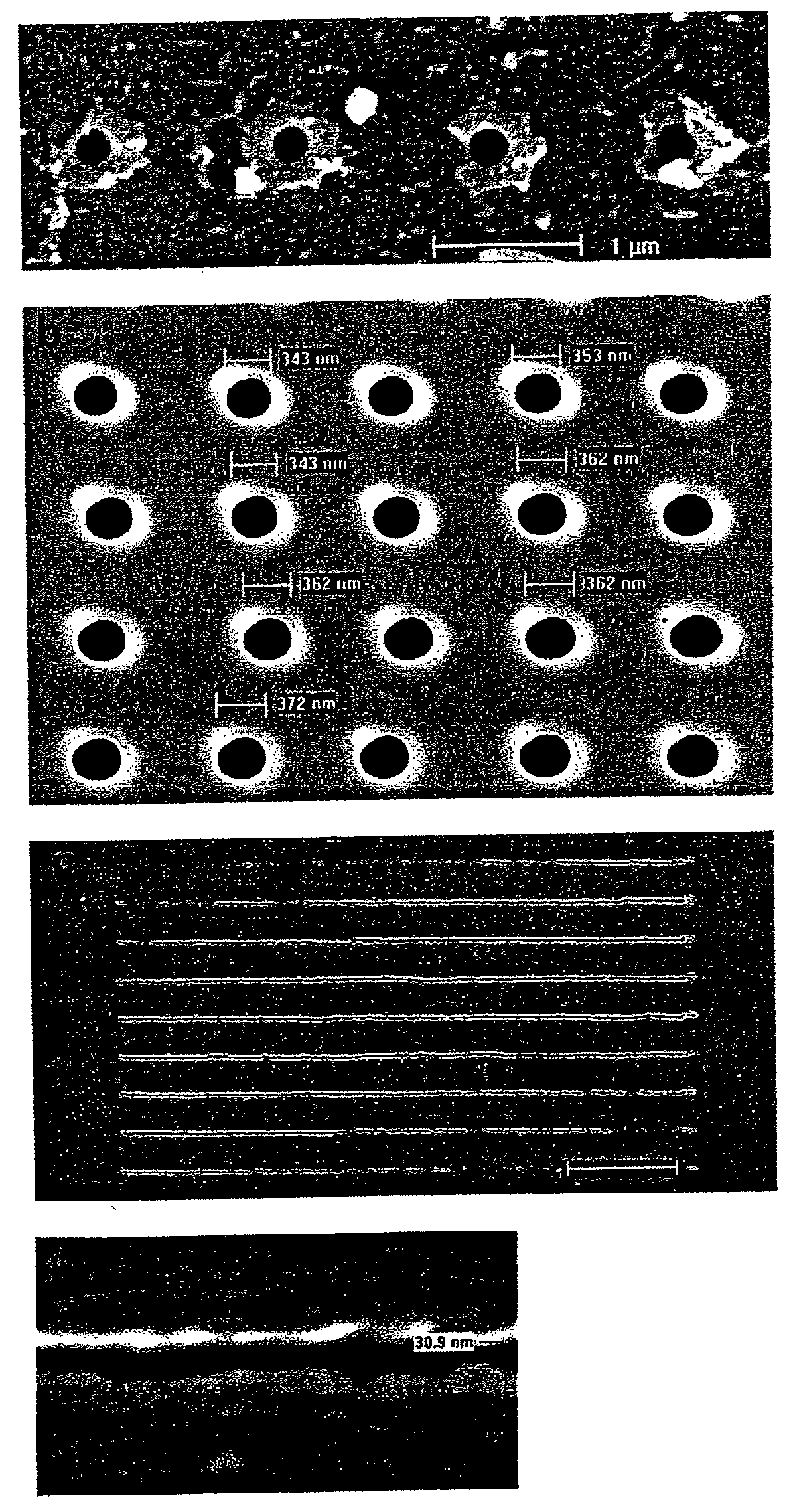
The present invention enables a new regime of robust, ultra-high-precision laser machining (UHPLM) where features are reduced by more than an order of magnitude. Here is presented a versatile technique for machining of nanometer-scale features using tightly-focused ultrashort laser pulses. By the invention, the size of features can be reduced far below the wavelength of light, thus enabling nanomachining of a wide range of materials. The features may be extremely small (<20 nm), are highly reproducible and are independent of the polarization of the light. This generalized process for nanoscale machining holds great promise for applications including MEMS construction and design, microelectronics, fabricating optical wave-guides and memory, microfluidics, materials science, microsurgery, and creating structures to interface with cells and biological molecules. The present invention will also anticipate significant impact in the biological sciences, enabling targeted disruption of nanoscale cellular structures and genetic material.
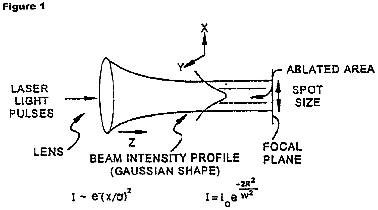
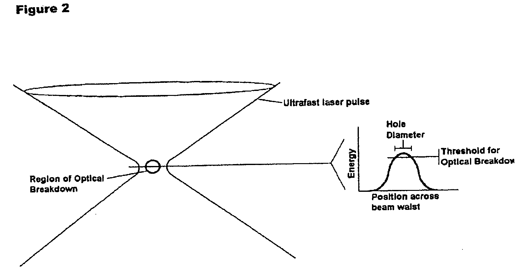
In one aspect, the method of the invention provides a laser beam which defines a spot that has a lateral gaussian profile characterized in that fluence at or near the center of the beam spot is greater than the damage threshold energy density whereby the laser induced breakdown is ablation of an area within the spot. The maximum intensity is at the very center of the beam waist. The beam waist is the point in the beam where wave-front becomes a perfect plane; that is, its radius of curvature is infinite. This center is at radius R=0 in the x-y axis and along the Z axis, Z=0. This makes it possible to damage material in a very small volume centered on Z=0, R=0. Thus it is possible to make features smaller than spot size in the x-y focal plane and smaller than the Rayleigh range (depth of focus) in the Z axis. It is preferred that the pulse width duration be in the femtosecond range although pulse duration of higher value may be used so long as the value is less than the pulse width defined by an abrupt or discernable change in slope of fluence breakdown threshold versus laser beam pulse width.
In still further variations, the structure's first passage may include one or more conduits in communication with a first group of grooves and a second passage has one or more conduits in communication with a second group of grooves. In a further feature, a first passage is constructed and arranged to provide flow communication between the grooves of the first groove set, and to prevent flow communication between the first groove set and the second groove set. A second passage provides flow communication between the grooves of the second groove set, and prevents communication between the first groove set and the second groove set. This encompasses a jumper arrangement where a groove of the second set is located between grooves of the first set.

Problems solved by technology

Radiation damage beyond the region of optical breakdown is insignificant because the extremely short duration of a pulse; the total energy delivered is negligible in regions where the intensity is insufficient to produce nonlinear events.

Method used


Image

  • Method for forming nanoscale features and structures produced thereby
  • Method for forming nanoscale features and structures produced thereby
  • Method for forming nanoscale features and structures produced thereby

Examples


Embodiment Construction

The following description of the preferred embodiment(s) is merely exemplary in nature and is in no way intended to limit the invention, its application, or uses.

The present invention provides a method to shape an optical pulse in space and time to achieve precise deterministic effects in smaller features heretofore not previously contemplated. See FIG. 4 of the present invention showing single spot and multiple spot patterns prepared by a single optical pulse shaped in space and time providing one or more regions of increased unbound electron density. In order to foster an understanding of the present invention developments, it is useful to understand principles associated with FIGS. 1, 2 and 3. FIGS. 1, 2 and 3 are schematic illustrations of a beam intensity profile showing that for laser micro-machining with ultrafast pulse, only the peak of the beam intensity profile exceeds the threshold intensity for ablation / machining.

FIG. 3 shows the radial and axial position on the beam...


PUM

PropertyMeasurementUnit
Lengthaaaaaaaaaa
Lengthaaaaaaaaaa
Lengthaaaaaaaaaa

Abstract

The invention provides a versatile technique for machining of nanometer-scale features using tightly-focused ultrashort laser pulses. By the invention, the size of features can be reduced far below the wavelength of light, thus enabling nanomachining of a wide range of materials. The features may be extremely small, of nanometer size, and are highly reproducible.

Description

FIELD OF THE INVENTION This invention relates generally to methods utilizing lasers for modifying internal and external surfaces of material such as by ablation or changing properties in structure of materials. This invention may be used for a variety of materials. BACKGROUND OF THE INVENTION Laser induced breakdown of a material causes chemical and physical changes, chemical and physical breakdown, disintegration, ablation, and vaporization. Lasers provide good control for procedures which require precision such as inscribing a micro pattern. Pulsed rather than continuous beams are more effective for many procedures, including medical procedures. A pulsed laser beam comprises bursts or pulses of light which are of very short duration, for example, on the order of 10 nanoseconds in duration or less. Typically, these pulses are separated by periods of quiescence. The peak power of each pulse is relatively high often on the order of gigawatts and capable of intensity on the order of...

Claims


Application Information

Patent Timeline
IPC IPC(8): B23K26/06B23K26/073B23K26/36
CPCB23K26/006Y10T428/24744B23K26/0635B23K26/0665B23K26/073B23K26/1417B23K26/36B23K26/365B23K26/381B23K26/4005B23K26/403B23K26/407B23K26/4075B23K2201/40B81C1/00492B82Y30/00B82Y40/00B81C2201/0143B23K26/121B23K26/1405B23K26/383Y10T428/24562Y10T428/24273B23K26/06B23K26/40B23K26/0624B23K26/1224B23K26/142B23K26/146B23K26/361B23K26/382B23K26/384B23K26/55B23K2101/40B23K2103/30B23K2103/50C03C23/0025
Inventor HUNT, ALAN J.HASSELBRINK, ERNEST F. JR.MEYHOFER, EDGARKE, KEVIN
Owner RGT UNIV OF MICHIGAN
Learn More