Apparatus and method of detecting the electroless deposition endpoint

a technology of electroless deposition and endpoint, which is applied in the direction of optical radiation measurement, semiconductor/solid-state device testing/measurement, instruments, etc., can solve the problems of affecting the reliability of connections, adding a great deal of complexity to the device forming process, and electroless deposition techniques that have not been extensively used for forming interconnects in vlsi and ulsi semiconductors

Inactive Publication Date: 2005-04-28
APPLIED MATERIALS INC
View PDF30 Cites 33 Cited by
  • Summary
  • Abstract
  • Description
  • Claims
  • Application Information

AI Technical Summary

Benefits of technology

[0024] Another aspect of the invention provides a method of controlling an electroless deposition process by emitting electromagnetic radiation from a broadband light source, detecting an intensity of the electromagnetic radiation at one or more wavelengths reflected off a surface of a substrate during an electroless deposition process at two or more positions on the surface of the substrate, comparing a detected electromagnetic radiation at a position on the surface of the substrate at a first time with the electromagnetic radiation at a second time and modifying a process step when the difference between the electromagnetic radiation at the position on the surface of the substrate at a first time and a second time exceeds a process value.
[0025] Another aspect of the invention provides a method of controlling an electroless deposition process by emitting electromagnetic radiation from a light source, detecting the intensity of reflected electromagnetic radiation off a surface of a substrate by use of a detector, scanning the detector across the surface of the substrate, calculating the average state of the process by summing the monitored intensities at one or more wavelengths over a period of time and dividing the summed results by the period of time, and modifying a process step when the calculated average intensity equals some process value.
[0026] Another aspect of the invention provides a method of controlling an electroless deposition process by emitting electromagnetic radiation from a light source, detecting the intensity of reflected electromagnetic radiation off a surface of a substrate at two or more wavelengths, calculating a difference in intensity of detected electromagnetic radiation intensity values at a first time and a second time at each detected wavelength, and monitoring the intensity of the electromagnetic radiation at a wavelength that has the largest calculated difference to determine the status of the electroless deposition process.
[0027] In another aspect of the invention an apparatus for monitoring an electroless deposition comprises a chamber, a substrate support disposed in the chamber having a substrate receiving surface, a substrate having a detection feature on a surface, wherein the substrate is disposed on the substrate receiving surface of the substrate support, an electromagnetic radiation source directed towards the surface of the substrate, a detector that detects the intensity of reflected electromagnetic radiation from the detection feature during an electroless deposition process, and a controller adapted to receive a signal from the detector and control the electroless deposition process.
[0028] Another aspect of the invention provides a method of controlling an electroless deposition process by positioning a substrate in an electroless deposition chamber, emitting electromagnetic radiation from a broadband light source onto a detection feature on the substrate, detecting an intensity of the electromagnetic radiation at one or more wavelengths that is reflected off the detection feature during an electroless deposition process step by use of a detector, and monitoring the intensity of the electromagnetic radiation at the one or more wavelengths to determine the status of the electroless deposition process.
[0029] Another aspect of the invention provides a method of controlling an electroless deposition process by positioning a substrate in an electroless deposition chamber, emitting electromagnetic radiation from a broadband light source onto the substrate, detecting an intensity of the electromagnetic radiation at one or more wavelengths that is reflected off a surface of a substrate at the start of the electroless deposition process by use of a detector, detecting an intensity of the electromagnetic radiation at one or more wavelengths that is reflected off a surface of a substrate at a second time by use of a detector, and modifying a process step when the change in the detected intensity at one or more wavelengths exceed a desired level.

Problems solved by technology

Even though copper has been selected as one of the favorite interconnection materials it has a couple drawbacks, since it is difficult to etch, it has a tendency to form a stable oxide layer when exposed to the atmosphere, and can form various corrosion products when exposed to other aggressive semiconductor fabrication environments.
The formation of the stable oxide layer can greatly affect the reliability of the connections.
The added steps of polishing, pattering and etching adds great complexity to the device forming process.
Although electroless deposition techniques have been widely used to deposit conductive metals over non-conductive printed circuit boards, electroless deposition techniques have not been extensively used for forming interconnects in VLSI and ULSI semiconductors.
Barrier layers comprising titanium, titanium nitride, tantalum, and / or tantalum nitride are poor surfaces for nucleation of a subsequently deposited conductive material layer, since native oxides of these barrier layer materials are easily formed.
One issue that arises with the use of an electroless deposition process is the effect that surface contamination or oxidation has on the time it takes the electroless deposition process to begin or “initiate.” This time, often known as the “initiation time,” is strongly dependent on the ability of the catalytic layer fluid or deposition fluid to interact with the surface of the interconnect feature.
However, since if there is no way to know when the process has initiated and the initiation time varies from substrate to substrate or from one area of a substrate to another it is hard to know when the desired thickness of material has been deposited across the surface of the substrate.
Use of a worst case process time causes the throughput of the deposition chamber to suffer and is wasteful of the often expensive electroless deposition solutions.
Also, variations in thickness of the deposited film across the surface of the substrate and / or the variations substrate-to-substrate will cause variations in the processing speed (e.g., propagation delay) of the formed devices.

Method used


Image

  • Apparatus and method of detecting the electroless deposition endpoint
  • Apparatus and method of detecting the electroless deposition endpoint
  • Apparatus and method of detecting the electroless deposition endpoint

Examples


Embodiment Construction

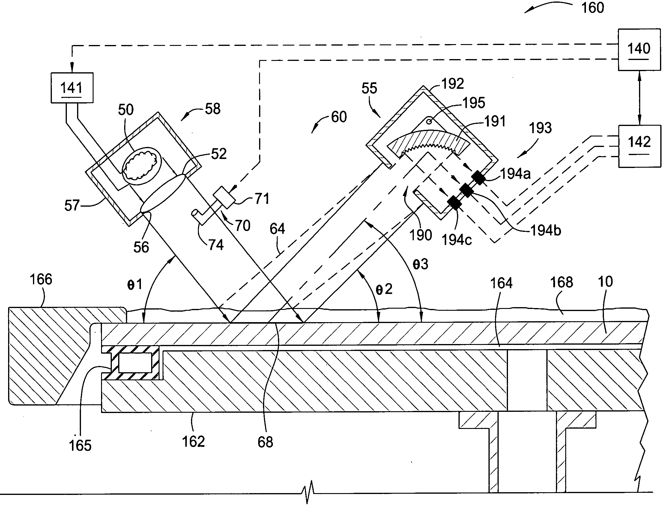
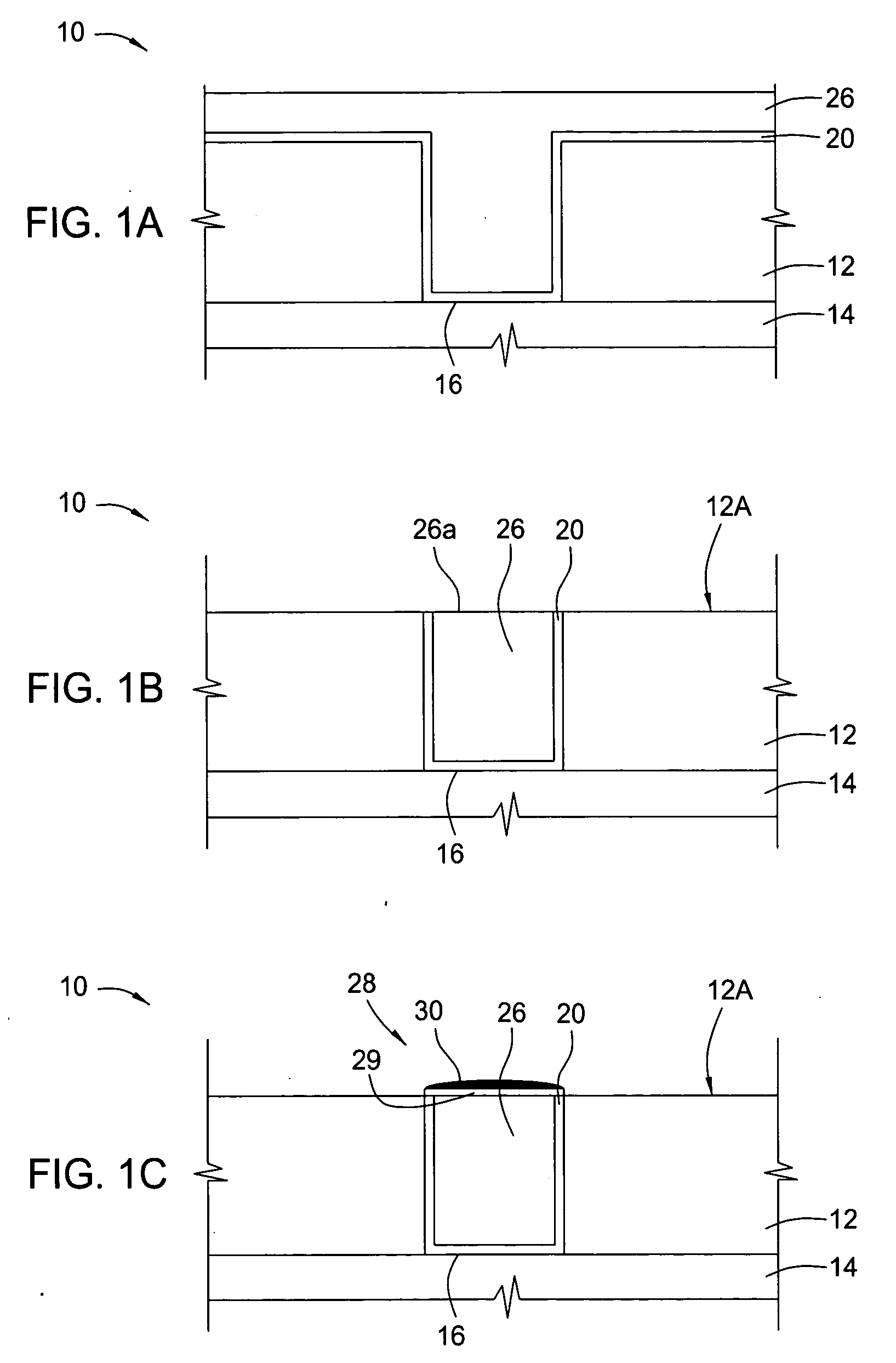
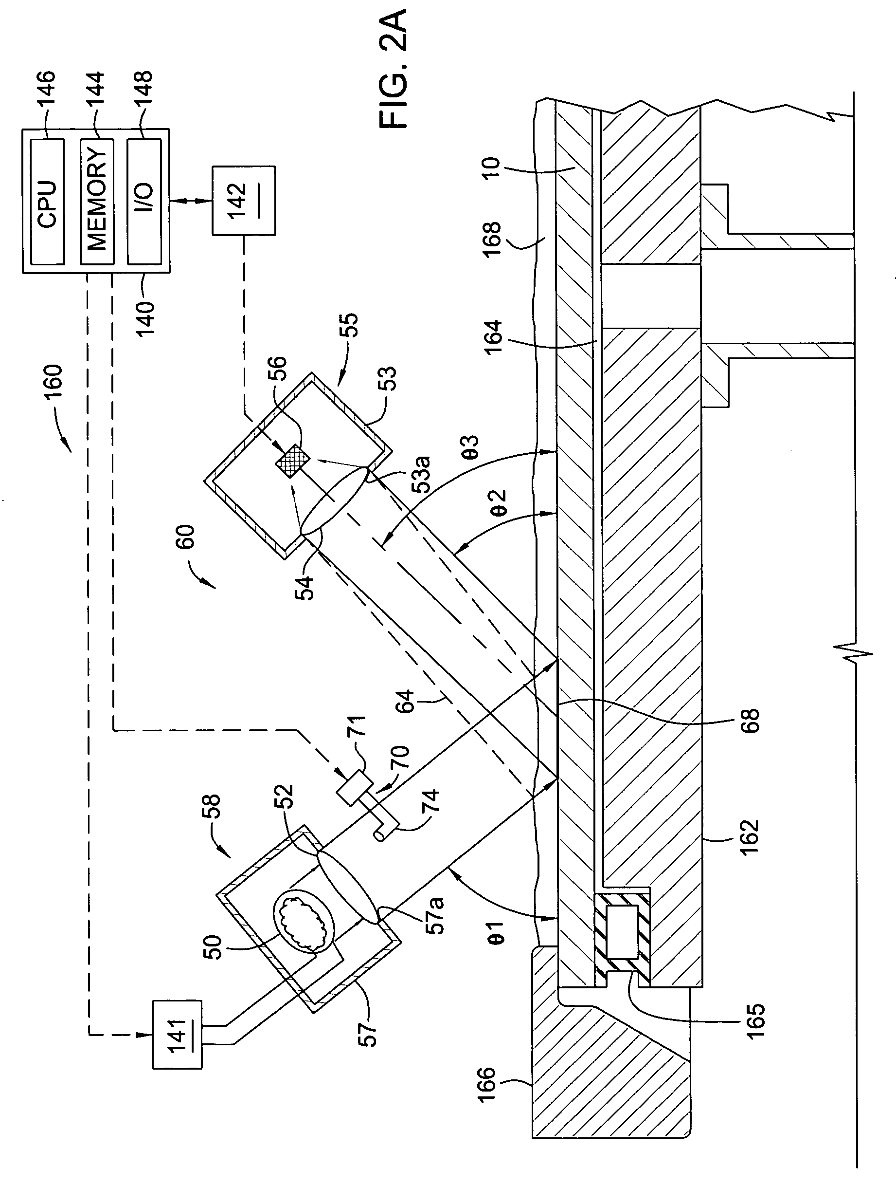
[0050]FIG. 1A shows a schematic cross-sectional view of a substrate base 14 formed on a substrate 10 and filled by a physical vapor deposition (PVD), Chemical vapor deposition (CVD), electrochemical deposition (ECP), electroless deposition, or a molecular beam epitaxy (MBE) process. The substrate 10 refers to any workpiece upon which film processing is performed. For example, the substrate 10 may be a silicon semiconductor substrate (or wafer), or other material layer that has been formed on the substrate. A dielectric layer 12 is deposited over the substrate. The dielectric layer 12 is generally an oxide, a silicon oxide, carbon-silicon-oxide, a fluoro-silicon, a porous dielectric, or other suitable dielectric. The dielectric layer 12 is patterned to provide a feature 16, such as a via, trench, contact hole, or line extending to an exposed surface portion of the substrate base 14. It is also understood by those with skill in the art that the present invention may be used in a dual ...


PUM

PropertyMeasurementUnit
wavelengthsaaaaaaaaaa
thicknessaaaaaaaaaa

Abstract

An apparatus and a method of controlling an electroless deposition process by directing electromagnetic radiation towards the surface of a substrate and detecting the change in intensity of the electromagnetic radiation at one or more wavelengths reflected off features on the surface of the substrate. In one embodiment the detected end of an electroless deposition process step is measured while the substrate is moved relative to the detection mechanism. In another embodiment multiple detection points are used to monitor the state of the deposition process across the surface of the substrate. In one embodiment the detection mechanism is immersed in the electroless deposition fluid on the substrate. In one embodiment a controller is used to monitor, store, and/or control the electroless deposition process by use of stored process values, comparison of data collected at different times, and various calculated time dependent data.

Description

CROSS-REFERENCE TO RELATED APPLICATIONS [0001] This application claims benefit of provisional U.S. Patent Application Ser. No. 60 / 503,833, filed Sep. 19, 2003, entitled “Apparatus and Method of Detecting The Electroless Deposition Endpoint,”[Attorney Docket No. 8651 L] and is herein incorporated by reference.BACKGROUND OF THE INVENTION [0002] 1. Field of the Invention [0003] The present invention generally relates to an apparatus and method of depositing a conductive material over sub-micron apertures formed on a substrate. [0004] 2. Description of the Related Art [0005] Reliably producing sub-micron and smaller features is one of the key technologies for the next generation of very large scale integration (VLSI) and ultra large scale integration (ULSI) semiconductor devices. However, as the boundaries of circuit technology are pressed, the shrinking dimensions of interconnects in VLSI and ULSI technologies have placed additional demands on the processing capabilities and consistent...

Claims


Application Information

Patent Timeline
Patent Type & Authority Applications(United States)
IPC IPC(8): C23C18/16G01B11/06G01J3/28G01N21/84G01N21/95H01L21/66
CPCC23C18/1651C23C18/1667G01N21/9501G01B11/0683G01N21/8422C23C18/1675C23C18/16G01B11/06
Inventor SHANMUGASUNDRAM, ARULKUMARBIRANG, MANOOCHERPANCHAM, IAN A.LOPATIN, SERGEY
Owner APPLIED MATERIALS INC
Why Eureka
Try Eureka