Devices having patterned regions of polycrystalline organic semiconductors, and methods of making the same

a polycrystalline organic semiconductor and semiconductor technology, applied in thermoelectric devices, nanoinformatics, transportation and packaging, etc., can solve the problems of inability to meet the requirements of harsh conditions, inability to withstand the harsh conditions of ambient temperature, rigid and brittle inorganic semiconductors, etc., to inhibit the nucleation of aromatic semiconductors, promote or inhibit crystal nucleation, and inhibit the effect of aromatic semiconductor nucleation

Inactive Publication Date: 2005-05-26
LUCENT TECH INC
View PDF21 Cites 20 Cited by
  • Summary
  • Abstract
  • Description
  • Claims
  • Application Information

AI Technical Summary

Benefits of technology

[0009] The present invention provides semiconductor apparatus in which patterned regions of a polycrystalline aromatic organic semiconductor are grown on a substrate. The patterning is directed by materials applied to the substrate to either promote or inhibit nucleation of crystals of the organic semiconductor. The material that promotes nucleation of the aromatic semiconductor comprises an aromatic moiety that can interact with the aromatic semiconductor. The exemplary material that inhibits nucleation of the aromatic semiconductor comprises a non-aromatic moiety or an aromatic moiety having insufficient conjugated pi-electrons to effectively interact with the aromatic semiconductor.

Problems solved by technology

In the absence of such patterning, the semiconductor devices may be inoperable or be subject to excessive crosstalk.
Inorganic semiconductors typically are rigid and brittle at ambient temperatures.
However, organic semiconductors generally cannot survive the harsh conditions required in order to carry out an etching step to generate a patterned array of channels for charge carrier transport.
However, in some cases the fine feature definition that is needed to generate microarrays of semiconductor channels has not been attained with acceptable reproducibility by direct printing of organic semiconductors.
However, tetracene thin film field effect transistors in general have low mobilities and on / off current ratios, and their integration into a circuit may require further development.
Furthermore, vacuum evaporation of tetracene leads to poorly defined and irregular boundaries between crystal grains that leads to low mobility and makes such grains unusable in fabricating semiconductor devices such as transistors or arrays comprising transistors.

Method used


Image

  • Devices having patterned regions of polycrystalline organic semiconductors, and methods of making the same
  • Devices having patterned regions of polycrystalline organic semiconductors, and methods of making the same
  • Devices having patterned regions of polycrystalline organic semiconductors, and methods of making the same

Examples


exemplary embodiment 100

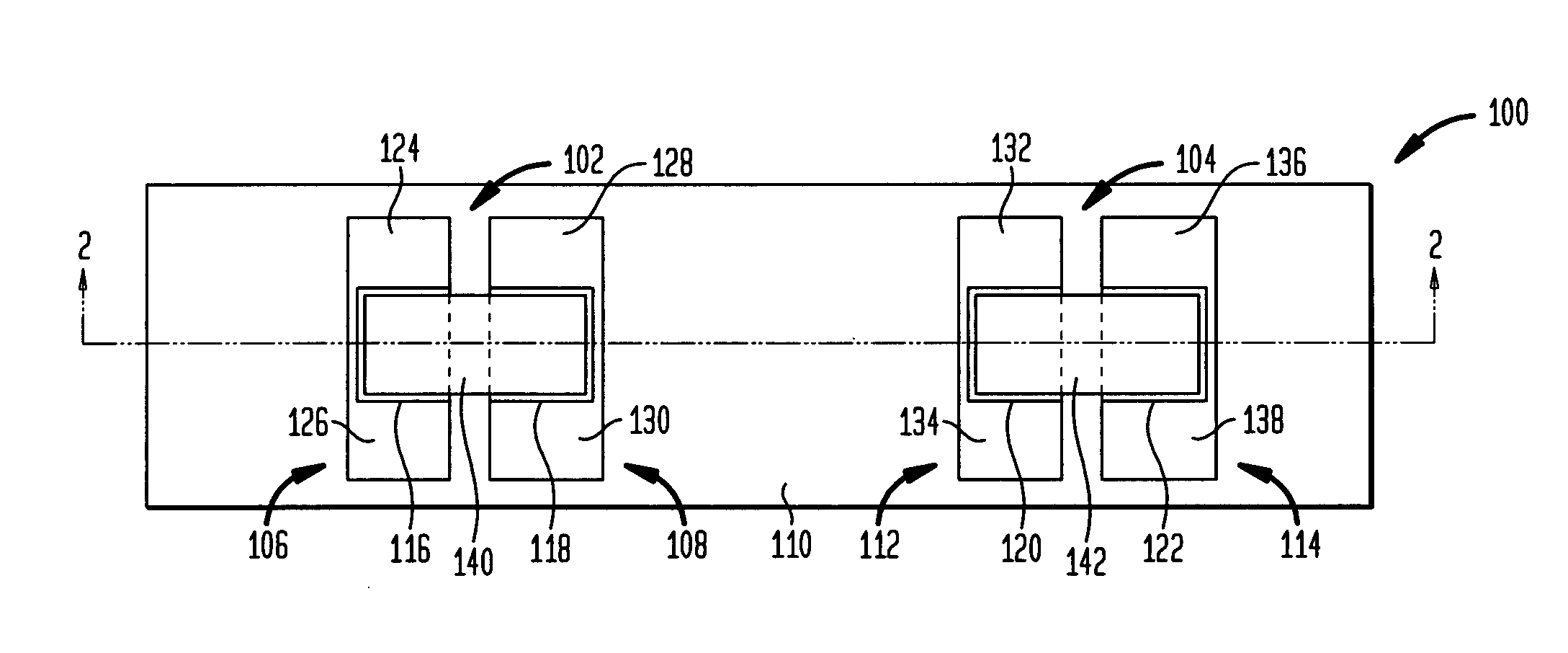
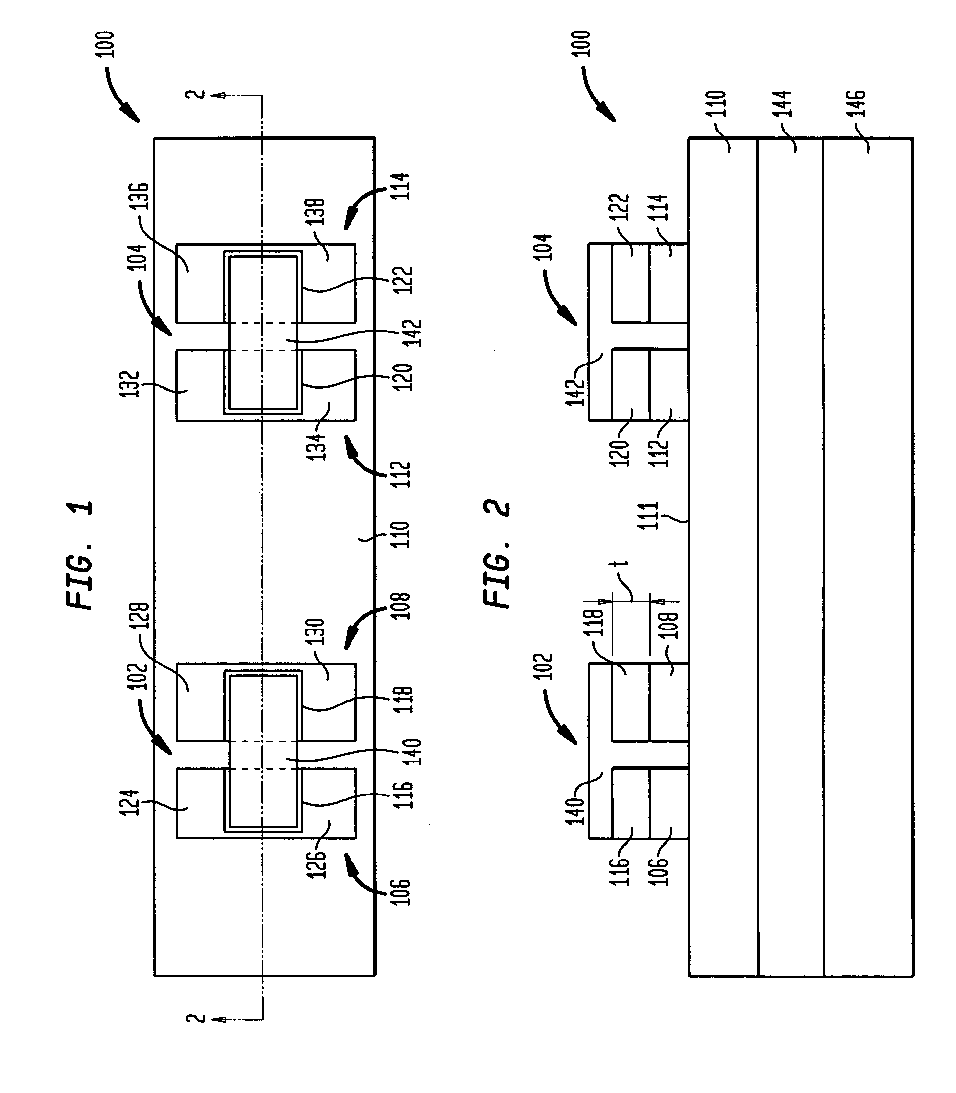
[0029]FIG. 1 shows an exemplary embodiment 100 of two thin film transistors generally indicated at 102 and 104. Thin film transistor 102 comprises a source electrode 106 and a drain electrode 108 in a spaced apart arrangement on a dielectric layer 110. The source electrode 106 and drain electrode 108 are fabricated from a composition to which a thiol moiety can bond, such as a composition comprising gold, silver, platinum, palladium, copper, or alloys of such elements. Thin film transistor 104 comprises a source electrode 112 and a drain electrode 114 fabricated from the same materials in a spaced apart arrangement on dielectric layer 110. A surface of each of the source electrodes 106 and 112 and of the drain electrodes 108 and 114 is centrally provided with semiconductor crystal nucleation augmentation regions 116, 120, 118 and 122, respectively constituted by a coating composition comprising a compound having a thiol moiety the electrodes and an aromatic moiety positioned to inte...

exemplary embodiment 300

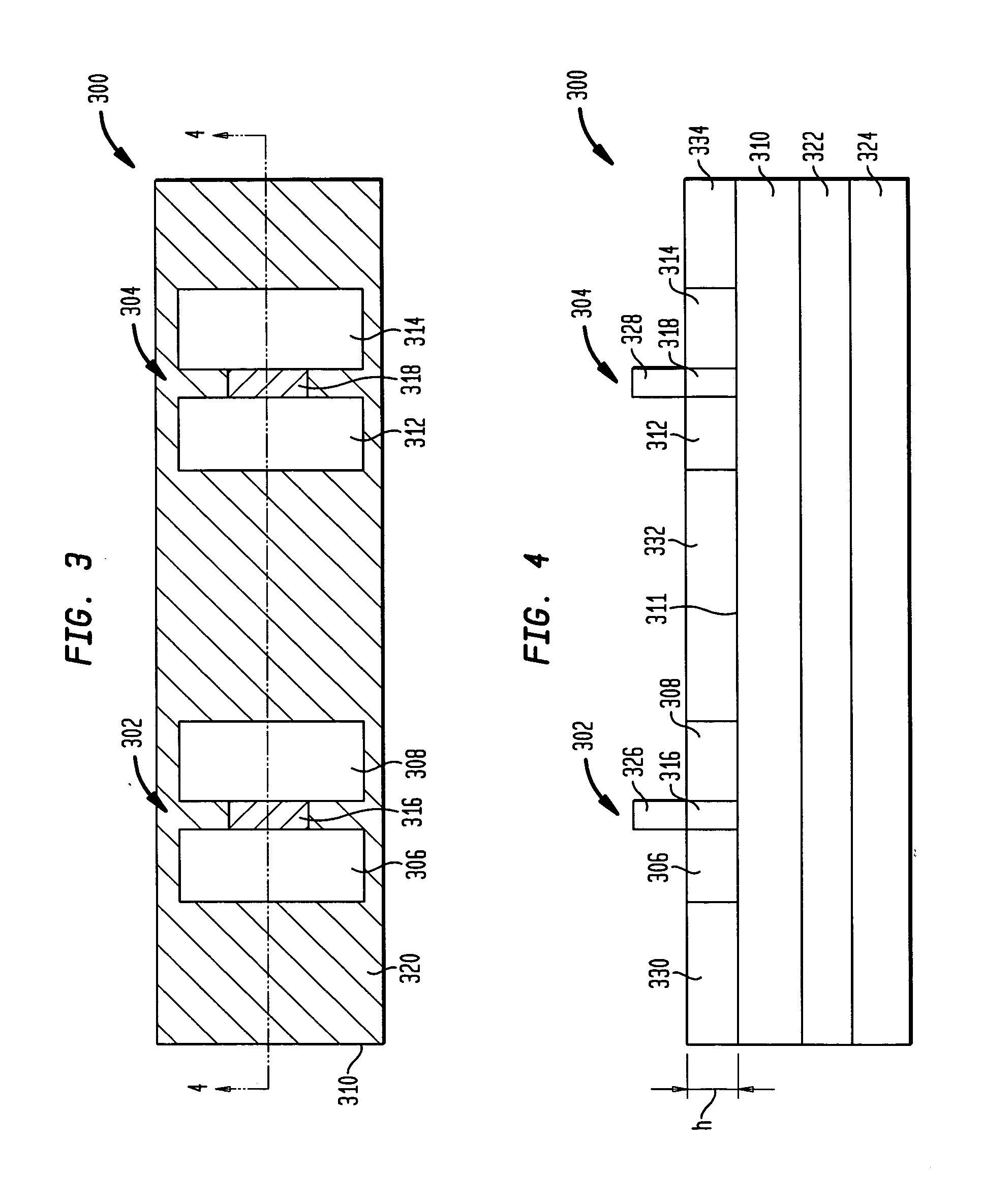
[0033]FIG. 3 shows an exemplary embodiment 300 of two thin film transistors generally indicated at 302 and 304. Thin film transistor 302 comprises a source electrode 306 and a drain electrode 308 in a spaced apart arrangement on a dielectric layer 310. Thin film transistor 304 comprises a source electrode 312 and a drain electrode 314 in a spaced apart arrangement on dielectric layer 310. Dielectric layer 310 is fabricated from a material comprising silicon, such as SiO2 or an alkyl siloxane. Siloxanes are compounds that have the general formula SiOR1R2R3, in which R1, R2, and R3 can each independently be selected from the group consisting of: Cl, —O—CH3, —O—CH2CH3, or R in which R is a hydrocarbon moiety such as an alkyl group for example. Background information regarding such dielectric layers is provided in Collet, J., et al., “High Anisotropic Conductivity in Organic Insulator / Semiconductor Monolayer Heterostructure,” Applied Physics Letters, Vol. 76, No. 10, pp. 1339-1341, Mar....

exemplary embodiment 500

[0040]FIG. 5 shows an exemplary embodiment 500 of two thin film transistors generally indicated at 502 and 504. Thin film transistor 502 comprises a source electrode 506 and a drain electrode 508 in a spaced apart arrangement on a semiconductor layer 510. Thin film transistor 504 comprises a source electrode 512 and a drain electrode 514 in a spaced apart arrangement on a semiconductor layer 516. Transistors 502 and 504 are supported by a dielectric layer 518 fabricated from a material comprising silicon, such as SiO2 or a siloxane.

[0041]FIG. 6 shows a cross-sectional view of the exemplary embodiment 500 of thin film transistors 502 and 504, taken on line 6-6 in FIG. 5. Source electrode 506 and drain electrode 508 of transistor 502 are on semiconductor layer 510. Source electrode 512 and drain electrode 514 of transistor 504 are on semiconductor layer 516. Semiconductor layer 510 is on semiconductor crystal nucleation augmentation region 520, such augmentation region constituted by ...


PUM


Abstract

Semiconductor apparatus comprising a substrate having a substrate surface; a first dielectric layer comprising molecules of a first compound, the molecules of the first compound having first ends and second ends, the first ends being covalently bonded to a first region of the substrate surface, the second ends having aromatic regions; and a polycrystalline semiconductor layer comprising organic semiconductor molecules with aromatic portions, the polycrystalline semiconductor layer being on the first region of the substrate. Integrated circuits comprising apparatus, and methods for making apparatus and integrated circuits.

Description

FIELD OF THE INVENTION [0001] The present invention relates to organic semiconductor devices and circuits containing organic semiconductor devices. BACKGROUND OF THE INVENTION [0002] Semiconductor devices are typically formed as multilayer structures in which the semiconductor materials are present in a patterned array that defines channels for the transport of charge carriers. For example, an inorganic semiconductor layer may be applied to a dielectric substrate surface. A mask may then be applied to protect patterned regions of the semiconductor layer, intended to constitute charge carrier channels, from a subsequently applied etchant. The etchant then removes the semiconductor in the unmasked regions, leaving behind a finely patterned array of semiconductor channels on the substrate. In the absence of such patterning, the semiconductor devices may be inoperable or be subject to excessive crosstalk. [0003] Inorganic semiconductors typically are rigid and brittle at ambient tempera...

Claims


Application Information

Patent Timeline
Patent Type & Authority Applications(United States)
IPC IPC(8): H01L21/336H01L27/28H01L51/05H01L29/786H01L51/30H01L51/40
CPCB82Y10/00B82Y30/00H01L51/0545H01L51/0004H01L51/0052H01L27/28Y10T428/31511Y10T428/31663H10K19/00H10K71/13H10K85/615H10K10/466
Inventor AIZENBERG, JOANNABAO, ZHENANBRISENO, ALEJANDRO L.HAN, YONG-JINMOON, HYUNSIK
Owner LUCENT TECH INC
Why Eureka
Try Eureka