
Removal of transition metal ternary and/or quaternary barrier materials from a substrate

a technology of ternary and/or quaternary barrier materials and transition metals, which is applied in the direction of coatings, chemical vapor deposition coatings, semiconductor devices, etc., can solve the problems of particle shedding, processing drift, and reaction that forms these films also occur non-productively on other exposed surfaces inside the processing chamber

Inactive Publication Date: 2005-05-26
VERSUM MATERIALS US LLC
View PDF9 Cites 269 Cited by
  • Summary
  • Abstract
  • Description
  • Claims
  • Application Information

AI Technical Summary

Problems solved by technology

While the deposition process desirably forms barrier films on a substrate (typically a silicon wafer), the reactions that form these films also occur non-productively on other exposed surfaces inside of the processing chamber.
Accumulation of deposition residues results in particle shedding, degradation of deposition uniformity, and processing drifts.
These effects can lead to wafer defects and subsequent device failure.
While there is a large body of work on etching tungsten metal, and dry cleaning of conventional CVD chambers used for depositing tungsten metal and other dielectric materials such as SiO2, these applications and processes are not directly applicable to transition metal ternary compounds such as tungsten-nitride-carbide (WNxCy) because these materials are much more chemically stable and highly refractory.
Furthermore, the incorporation of carbon into certain transition metal ternary materials poses additional challenges.
Such a problem has become well known in etching and cleaning of carbon-doped silicate glass (CSG) low dielectric constant materials.
Mechanical and wet clean processes are time consuming and labor intensive.

Method used


Image

  • Removal of transition metal ternary and/or quaternary barrier materials from a substrate
  • Removal of transition metal ternary and/or quaternary barrier materials from a substrate
  • Removal of transition metal ternary and/or quaternary barrier materials from a substrate

Examples


example 1

Remote Plasma Cleaning of Ternary Tungsten Nitride Carbide (WNxCy) Materials

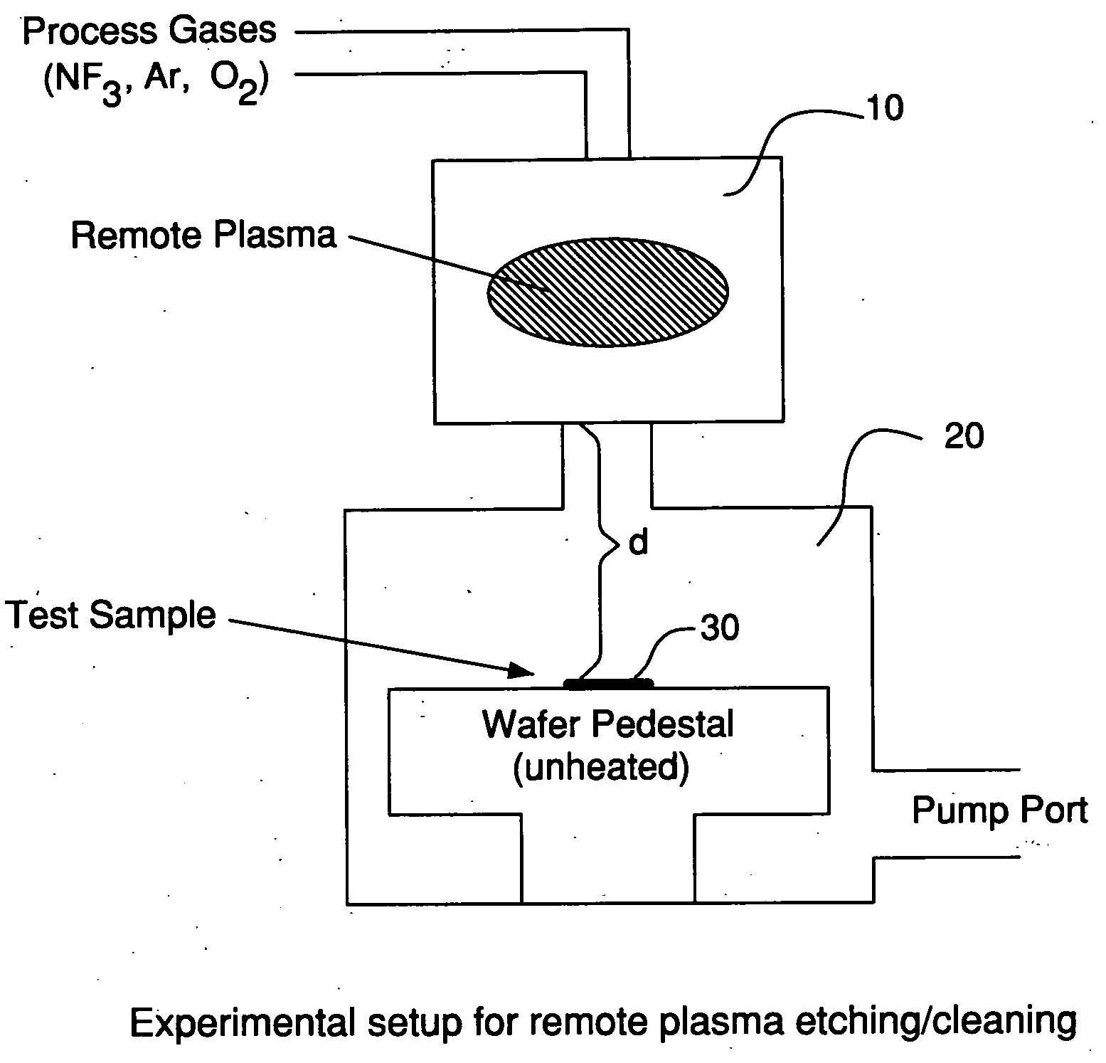
[0040]FIG. 1 provides an illustration of the experimental setup for remote plasma cleaning. An ASTRON® remote plasma generator 10 manufactured by MKS Instruments of Wilmington, Mass. was mounted on top of process chamber 20. The distance “d” between the exit of remote plasma generator 10 and the sample coupon 30 is about six inches. Table 1 lists the experiment recipes and WNxCy etch rates. In all of the runs, the chamber pressure was kept at 4 Torr. The thickness of the tungsten nitride carbide layer on the sample coupon is about 90 nm.

[0041] Each run was conducted in the following manner: vent chamber and open front door; load sample coupons and close front door; evacuate chamber to reach baseline vacuum pressure; introduce argon (Ar) gas and stabilize pressure; turn on the remote plasma power; introduce process gases; turn off the remote plasma power after 1 minute; stop process flows and evacuate chamb...

example 2

In Situ Plasma Cleaning of WNxCy

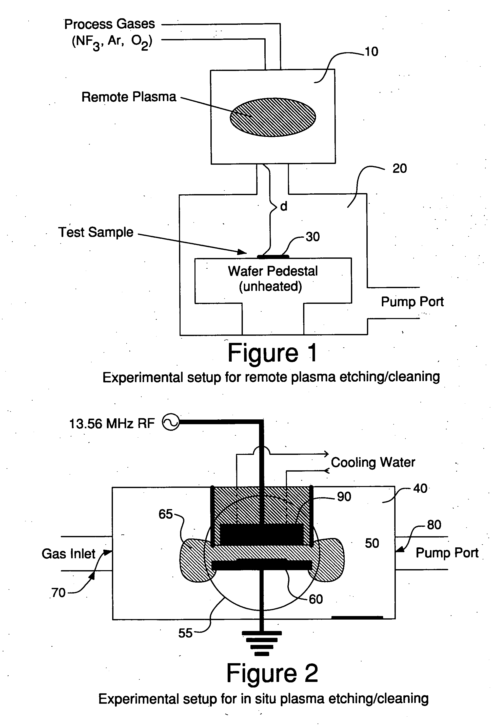
[0042]FIG. 2 provides an illustration of the experimental setup for in situ plasma cleaning of WNxCy. The experiments were run in a capacitively coupled parallel plate process chamber 40. The gap spacing between the two electrodes was one inch. A sample coupon 50 was placed on the center of the grounded lower electrode 60 so that it is in direct contact with the plasma. There is no dc self-bias voltage and no RF driven voltage at grounded electrode and chamber walls. Process gases were introduced from a side port 70 and pumped out through another port 80 on the opposite side of the chamber. RF power was applied to the top electrode 90, which was water cooled at 20° C. The thickness of the tungsten nitride carbide layer on the sample coupon is about 20 nm.

[0043] Each run was conducted in the following manner: process chamber 40 was loaded with sample coupons 50 and sample loading door 55 was closed. Chamber 40 was evacuated to reach baseline vacuum p...

example 3

Thermal NF3 Cleaning of WNxCy

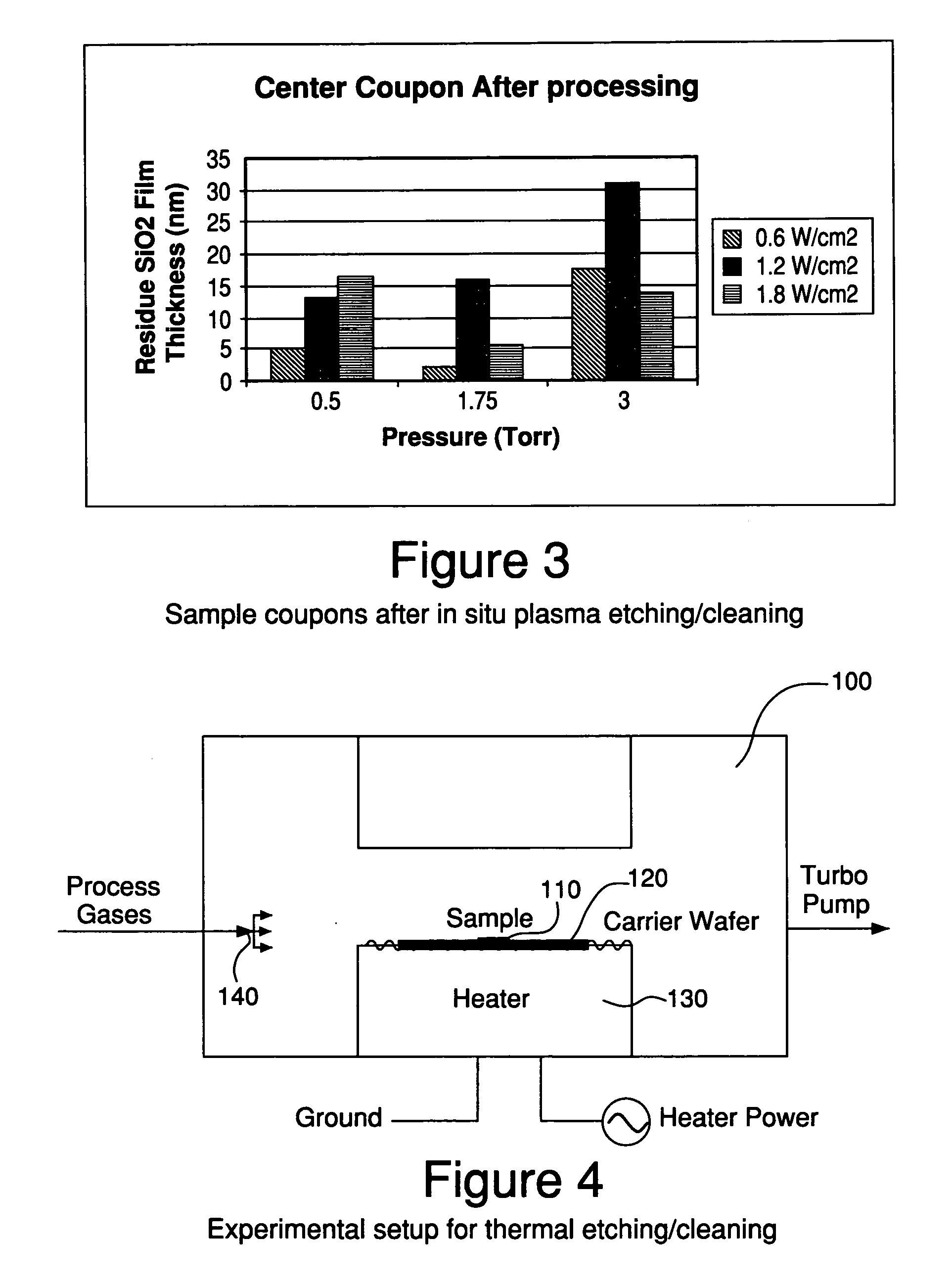
[0046]FIG. 4 is a schematic diagram of the experimental setup for thermal clean of WNxCy sample coupons. This process chamber 100 was modified from the in situ plasma process chamber 40 shown in FIG. 2. The sample coupon 110 was placed on a 4 inch carrier wafer 120, which was placed on a heated pedestal 130. Other aspects of the process chamber design were similar to those described in FIG. 2. After the introduction of the sample coupon and evacuation of the process chamber, the pedestal and the sample coupon was heated by a resistive heater to reach a preset temperature. A process gas 140 containing the fluorine-containing gas NF3 was then fed into the process chamber 100 to reach a preset chamber pressure to remove the WNxCy film from the sample coupon 110. The sample coupons were measured by spectroscopic ellipsometer before and after the processing. The thickness of the tungsten nitride carbide layer on the sample coupon is about 20 nm. Table 2 list...


PUM

PropertyMeasurementUnit
thicknessaaaaaaaaaa
thicknessaaaaaaaaaa
temperatureaaaaaaaaaa

Abstract

A process for the selective removal of a substance from a substrate for etching and / or cleaning applications is disclosed herein. In one embodiment, there is provided a process for removing a substance from a substrate comprising: providing the substrate having the substance deposited thereupon wherein the substance comprises a transition metal ternary compound, a transition metal quaternary compound, and combinations thereof; reacting the substance with a process gas comprising a fluorine-containing gas and optionally an additive gas to form a volatile product; and removing the volatile product from the substrate to thereby remove the substance from the substrate.

Description

CROSS-REFERENCE TO RELATED APPLICATIONS [0001] This application claims the benefit of U.S. Provisional Application No. 60 / 507,224, filed 30 Sep. 2003.BACKGROUND OF THE INVENTION [0002] In recent years, the semiconductor industry has widely adopted copper or copper-containing compounds as conductive materials and low dielectric constant (low-k) materials as insulating materials for interconnection between transistors in integrated circuit (IC) manufacturing. One manufacturing step that helps ensure the successful integration of copper and low-k dielectric materials is the deposition of barrier materials between copper and dielectric materials. The barrier materials may also be called diffusion barrier or liner materials. Barrier materials may serve both as a diffusion barrier that prevents the diffusion or migration of the conductive materials into the insulating materials and active regions of transistors, and as an adhesion promoter that eliminates delamination and voids between th...

Claims


Application Information

Patent Timeline
Patent Type & Authority Applications(United States)
IPC IPC(8): C23C16/44C23G5/00H01L21/302H01L21/3213H01L21/44H01L21/461
CPCC23C16/4405H01L21/32136H01L21/32135C23G5/00Y10S438/905
Inventor JI, BINGPLISHKA, MARTIN JAYWU, DINGJUNBADOWSKI, PETER RICHARDKARWACKI, EUGENE JOSEPH JR.
Owner VERSUM MATERIALS US LLC
Learn More