Molecular modifications of metal/dielectric interfaces

a technology of dielectric interface and metal, which is applied in the direction of semiconductor devices, electrical apparatus, nanotechnology, etc., can solve the problems of non-zero values of eot/sub>gate, change in the effective sub>m/sub> of metals, etc., and achieve the effect of improving the electrical characteristics of mim or mis structures

Inactive Publication Date: 2005-06-16
ARIZONA BOARD OF GEGENTS ACTING FOR & ON BEHALF OF ARIZONA STATE UNIV +1
View PDF13 Cites 14 Cited by
  • Summary
  • Abstract
  • Description
  • Claims
  • Application Information

AI Technical Summary

Benefits of technology

[0011] In another embodiment, there is a method of improving the electrical characteristics of MIM or MIS structures that includes providing a metal surface and contacting the metal surface with a solution of at least one selected biochemical having a permanent dipole moment and being capable of self assembly for a sufficient time for the biochemical to self assemble molecularly (SAM) on the metal surface. The SAM can be aminopropyl triethoxy silane, fatty acids, organosilicon derivatives, organosulfur compounds, alkyl chains, diphosphates or a combination thereof. The metal can be at least one of Ta, Ti, Ni, Co, W, Mo, Ru, Ir, Pt, Al, Cr, Pd, Re, Ar or Ha. Before the contacting step, there can be another step of activating molecules on the metal surface.

Problems solved by technology

The production of such dual-metal MOSFETs will not only introduce additional process complexities (deposition / etching) and issues of yield, the potential for interfacial reactions of low electronegativity metals with high K dielectrics could lead to non-zero values of EOTgate, as well as a change in the effective φm of metals.

Method used


Image

  • Molecular modifications of metal/dielectric interfaces
  • Molecular modifications of metal/dielectric interfaces
  • Molecular modifications of metal/dielectric interfaces

Examples


example 2

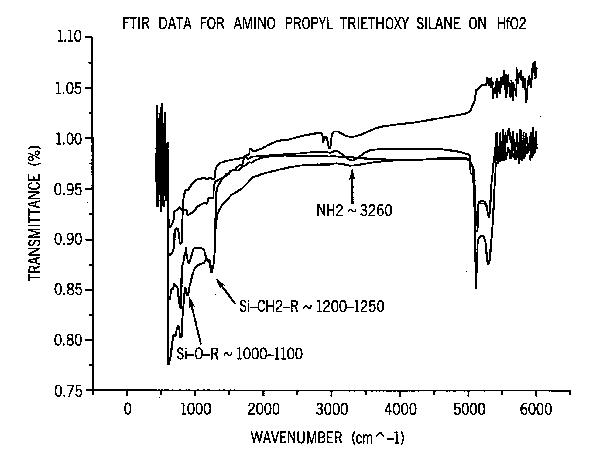
[0024] The binding of SAMs on an oxide surface was confirmed by using Fourier-transform infrared spectroscopy (FTIR). Shown in FIG. 1 are FTIR spectra of APTES deposited on ALD-HfO2 of three different thicknesses, 40 Å, 60 Å, and 90 Å. FIG. 1 also shows a reference FTIR spectrum of a bare ALD-HfO2 surface. The arrows indicate the vibrational energy levels for the important bonds: NH2 (3260 cm−1), Si—(CH2)3(1200-1250 cm−1), and Si—O—C2H5 (1000-1100 cm−1).

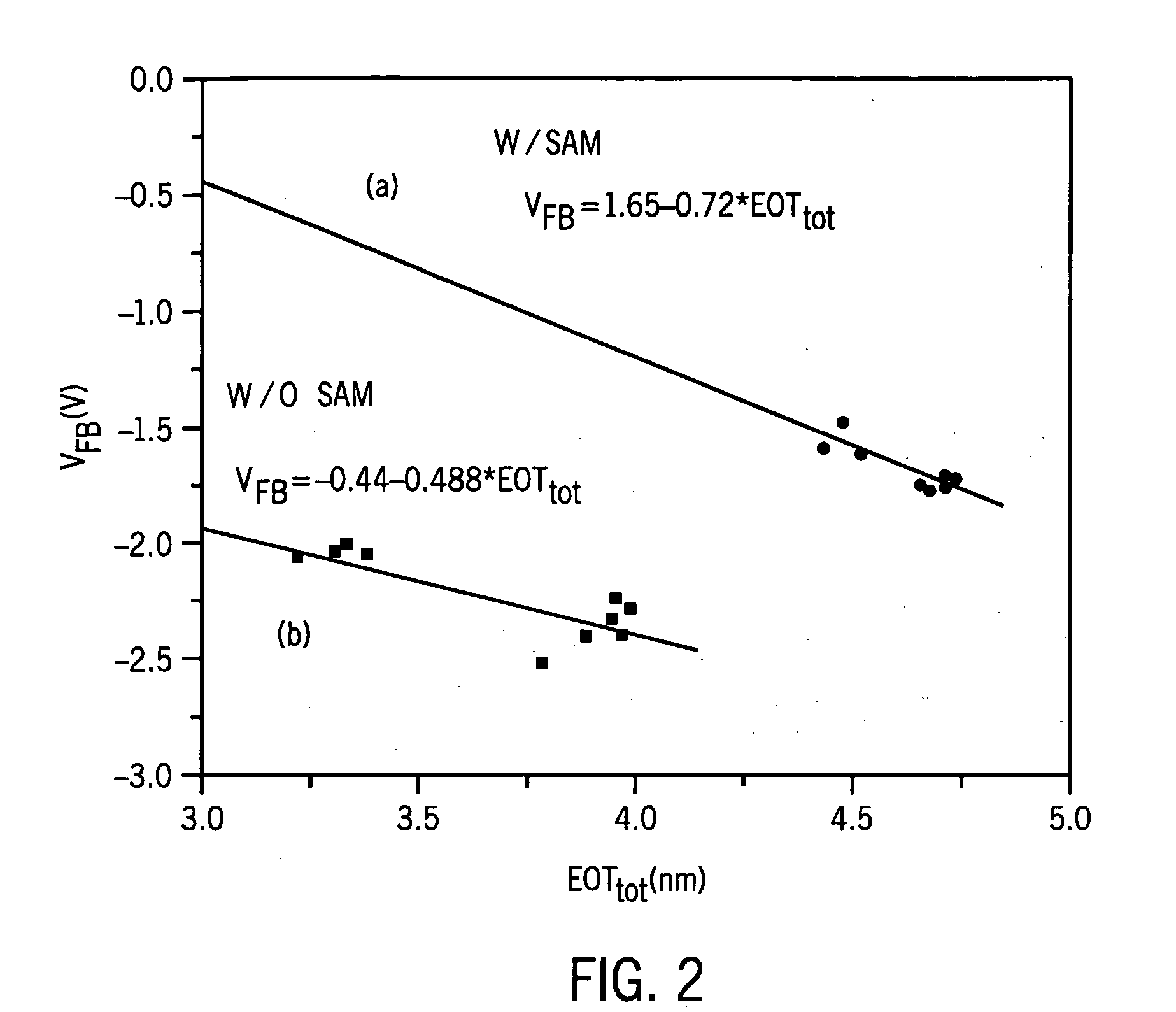
[0025] In order to estimate the work-function of an aluminum (Al) electrode, the equivalent oxide thickness (EOT) and the flat-band voltage (VFB) were calculated from C-V plots in the Al / SAM / HfO2 / SiO2 / p+-Si configuration for different thicknesses of ALD-HfO2. FIG. 2 illustrates the plots of VFB versus EOT before and after modification of the AL / HfO2 interface by SAM. The slope of the fitted linear-line corresponds to a fixed-charge density (Nf). If it were assumed that Nf is located at SiOx / Si interface, the intercept corresponds to...

example 3

[0026] A method commonly known as silanization was used to deposit SAM onto thermal SiO2 / Si surfaces with a 4 nm SiO2 thickness (tSiO2); followed by Ti metal top-electrode deposition by e-beam evaporation. With saturated surface coverage of SAM, the φm of Ti was determined through capacitance-voltage (C-V) analysis. The binding of SAM on SiO2 was confirmed by using Fourier-transform infrared spectroscopy (FTIR) and surface coverage of SAM was determined by the change in VFB with deposition time.

[0027] Substrate Preparation: The SiO2 layers (with a thickness tSiO2 of 4, 6, and 8 nm) were deposited on Si by a thermal oxidation process at International Sematech (Austin, Tex.). Prior to the deposition of SAM, the removal of organic deposits on these SiO2 / Si wafers was carried out by rapid thermal annealing (RTA) at 350° C. for 1 minute using a AG Associates (San Jose, Calif.) Heat Pulse 610, followed by sonication with 70% isopropyl alcohol (in water) for 30 sec and then with acetone f...


PUM


Abstract

A method of increasing the work function of micro-electrodes includes providing a metal or silica surface functionalized with reactive groups and contacting the functionalized surface with a solution of at least one biochemical, having a permanent dipole moment and being capable of self assembly, for a sufficient time for the biochemical to self assemble molecularly (SAM) on the functionalized surface. The biochemical can be aminopropyl triethoxy silane, fatty acids, organosilicon derivatives, organosulfur compounds, alkyl chains, or dihosphates. Use in a wide variety of metals and metallic compounds is disclosed.

Description

CLAIM TO DOMESTIC PRIORITY [0001] The present non-provisional patent application claims the benefit of provisional application Ser. No. 60 / 525,281 entitled “Molecular Modifications of Metal / Dielectric Interfaces”, filed on Nov. 25, 2003.FIELD OF THE INVENTION [0002] The present invention relates in general to modifying metal / insulator, metal / semiconductor, and metal / metal interfaces for the purpose of molecular electronics and biodevices and more specifically to biochemical deposition on such interfaces to increase the work function of the interface. BACKGROUND OF THE INVENTION [0003] The use of organic molecules to modify the interface between metal and high-permittivity (K) material is a recent development that has a wealth of potential applications in microelectronics, optoelectronics and in the rapidly growing area of molecular electronics and bio-nanodevices. In terms of molecular control over electronic device properties, there have been two main approaches a) control of the e...

Claims


Application Information

Patent Timeline
Patent Type & Authority Applications(United States)
IPC IPC(8): H01L51/00H01L51/30H01L51/40
CPCB82Y10/00H01L51/0595H01L51/0075H01L51/0021H10K71/60H10K85/701H10K10/701
Inventor DEY, SANDWIP K.SISTIABUDI, RIZALDIGU, DIEFENGGOSWAMI, JAYDEB
Owner ARIZONA BOARD OF GEGENTS ACTING FOR & ON BEHALF OF ARIZONA STATE UNIV
Why Eureka
Try Eureka