[0024] The present invention has been made in view of the above problems, and it is therefore an object of the invention to provide a semiconductor readout circuit capable of effectively reading out memory
cell data at a high speed even in the case where capacity and resistance of a bit line are large.
[0027] According to the semiconductor readout circuit of the present invention, even in the case where the precharge period is continued even after completion of charging of the bit lines, start of a period when the
load circuit is made inactive is set to at latest upon or in the vicinity of a time when the charging of the bit lines is completed, so that the readout input node can be prevented from being charged to an unnecessarily
high voltage from the level upon completion of the charging of the bit lines. If the precharge period is completed before or after a timing when the word line selects a memory cell to be read out and, then, a cell current of the memory cell, i.e., a bit
line current is flown out via the selected bit line, the load circuit is made active at the same timing, so that it is possible to shift to the voltage of the readout input node according to the cell current corresponding to the memory state of the memory cell at a high speed.
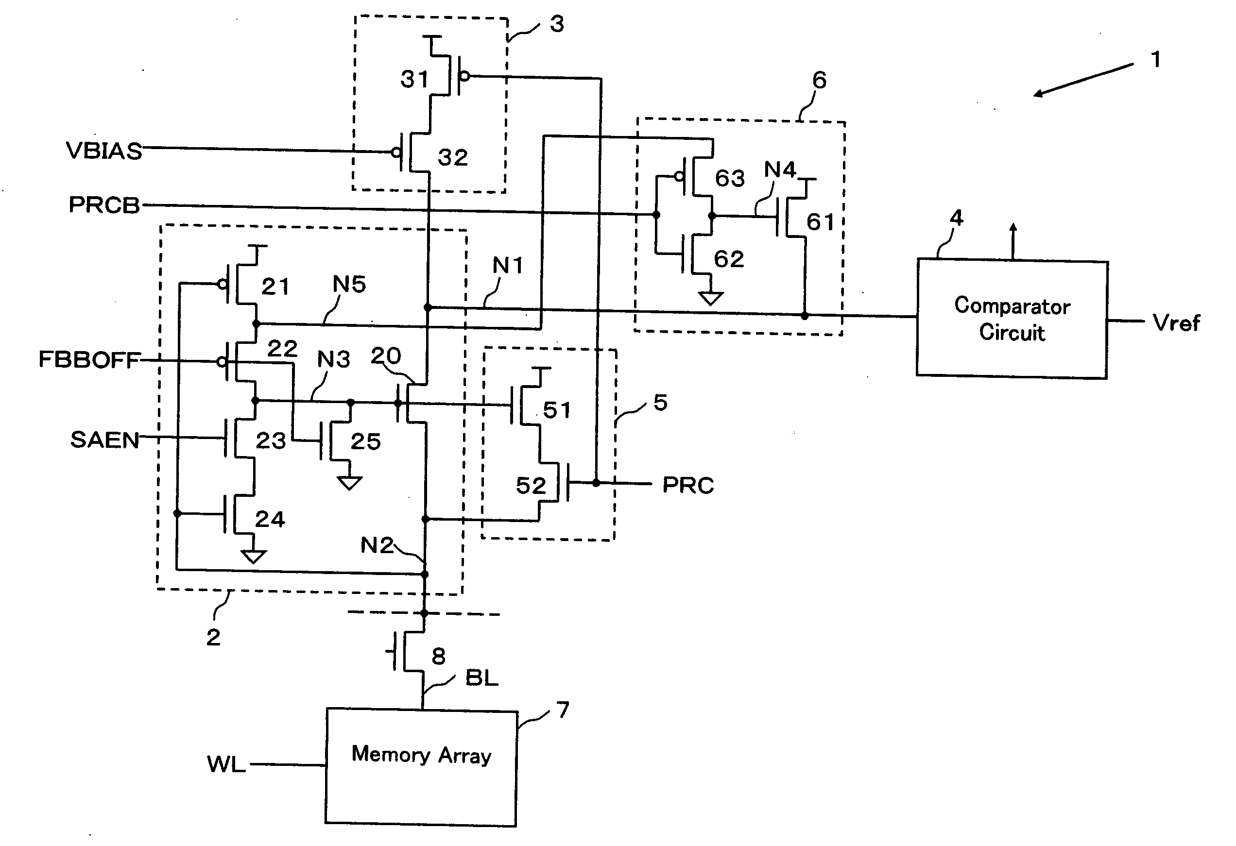
[0029] According to the second aspect of the present invention, when the
reference cell is set to have an intermediate current within a fluctuation range of the cell current of the memory cell, the reference voltage can be set to have an intermediate voltage value within a fluctuation range of the voltage of the readout input node. In addition, when the
comparator circuit compares the reference voltage with the voltage of the readout input node as differential inputs, it is possible to reliably perform a readout operation of a memory cell corresponding to an amount of cell currents of the memory cell at a high speed. In particular, when the reference voltage generation circuit is designed to have the same configuration as those of the circuits in a readout
system from a charge circuit to a memory cell, an operation margin can be maintained widely because the reference voltage and the voltage of the readout input node change according to changes in an operation voltage, an
operation temperature, variation of a manufacturing process and the like.
[0031] According to a third aspect of the present invention, the semiconductor readout circuit according to the first or second aspect further comprises a hold circuit which holds the voltage of the readout input node at a predetermined hold voltage during, at least, the load circuit is inactive. According to the third aspect of the present invention, the voltage of the readout input node in a period before the bit
line current flows and the memory cell readout starts after completion of charging of the bit line, can be set at an optimal level for operations of the
sense amplifier at the subsequent stage thereof. As a consequence, after the bit
line current starts flowing, the
sense amplifier can carry out a high speed output operation according to voltage changes of the readout input node corresponding to an amount of cell currents.
[0034] According to the fourth aspect of the present invention, since the amount of currents of the P-type
MOSFET is within a range of the memory cell currents, when the bit line current flows and the load circuit is made active, an amount of load currents of the lord circuit does not excessively become large or small with respect to the memory cell current, so that the voltage of the readout input node can promptly shift to a voltage value according to an amount of memory cell currents. Thus, the above configuration contributes to a high-speed readout operation of the sense
amplifier.
[0037] According to the fifth aspect of the present invention, when the dummy bit line is structured by suitably simulating parasitic capacity or parasitic resistance of the bit line, the following effects can be exhibited: a charging state of the bit line can be monitored by a change in voltage of the dummy bit line, termination of the precharge period when the precharge circuit is active can be automatically set at a completion timing of charging of the bit line, and a memory cell readout operation can be promptly performed after completion of charging of the bit line. Consequently, it is possible to promote a high-speed readout operation of a voltage of the readout input node by the sense
amplifier. Basically, parasitic capacity and parasitic resistance of a dummy bit line is equivalent to those of the bit line. However, when the timing adjustment of the precharge period is needed, by adjusting the parasitic capacity and parasitic resistance of the dummy bit line, i.e., the length of the dummy bit line and the number of dummy memory cells to be connected, the timing can be adjusted.

