Magnetic memory device and manufacturing method thereof
Inactive Publication Date: 2005-07-28
SONY CORP
View PDF11 Cites 8 Cited by
- Summary
- Abstract
- Description
- Claims
- Application Information
AI Technical Summary
Benefits of technology
[0014] The first magnetic memory device mentioned above has a magnetic flux concentrator of high-permeability layer formed at least on the lateral sides of a first wiring and on the side of the first wiring which is opposite to the side facing the tunnel magnetoresistance element. At least either of the high-permeability layer formed on the lateral sides of the first wiring projects from the first wiring toward the tunnel magnetoresistance element. Therefore, the magnetic field generated by the first wiring is efficiently concentrated at the memory layer of the tunnel magnetoresistance element by part of the magnetic flux concentrator projecting toward the tunnel magnetoresistance element. The effect of the foregoing is that it is possible to reduce the current value necessary for writing. This leads to the saving of power consumption and extends the life on electromigration of the first wiring. The reduction of driving current permits the area of the current driving circuit to be reduced, which in turn leads to a higher degree of integration. Moreover, the reduced driving current decreases the leakage of magnetic field, thereby decreasing interference effect with adjacent cells.
[0037] The method of producing the sixth magnetic memory device mentioned above includes a step of forming a magnetic flux concentrator of high-permeability layer at least on the lateral sides of the second wiring and on the side of the second wiring which is opposite to the side facing the tunnel magnetoresistance element. At least either of the high-permeability layers formed on both of the lateral sides of the second wiring projects from the second wiring toward the tunnel magnetoresistance element. Therefore, as in the method of producing the second magnetic memory device, the magnetic field generated by current flowing through the second wiring is efficiently concentrated at the memory layer (or recording layer) of the tunnel magnetoresistance element. The effect of the foregoing is that it is possible to reduce the current value necessary for writing. This leads to the saving of power consumption and extends the life on electromigration of the second wiring. The reduction of driving current permits the area of the current driving circuit to be reduced, which in turn leads to a higher degree of integration. Moreover, the reduced driving current decreases the leakage of magnetic field, thereby decreasing interference effect with adjacent cells.
Problems solved by technology
Moreover, non-volatile memory with a higher recording density and a larger recording capacity is expected to replace the existing hard disks and optical disks, which are essentially limited in further miniaturization, containing moving parts.
Flush memory is limited in writing speed (of the order of microseconds).
FRAM is limited in rewriting cycles 1012 to 1014 and hence is low in durability to displace to SRAM (Static Random Access Memory) and DRAM (Dynamic Random Access Memory).
Moreover, FRAM encounters difficulties in microprocessing of ferroelectric capacitors.
Unfortunately, they have the disadvantage that the memory cell has a low resistance of 10 to 100 Ω, which leads to a large power consumption per bit for reading.
This disadvantage makes it difficult to realize a large-capacity memory.
Unfortunately, the advantage of MRAM, which is high speed and large integration as mentioned above, is offset by high power consumption due to MRAM's inherent structure.
High power consumption is contrary to power saving required of portable equipment.
Moreover, MRAM involves problems with large integration, because the bit lines and writing word lines should have the minimum line width determined by the lithography technology.
This current density is large enough to pose problems with short life due to electromigration, even though the bit lines and word lines are made of copper (whose practical current density is 0.5 MA / cm2).
This poses a serious problem with wiring reliability.
Further, large integration is impeded, because the bit lines and writing word lines need high-current drivers occupying large areas.
In addition, greatly miniaturized element causes the leakage of magnetic flux, which generates the magnetic field in adjacent bits.
This poses a problem with disturbance.
The claimed measure, however, does not fully produce the effect of concentrating magnetic flux and hence does not reduce power consumption as expected.
Method used
View moreImage
Smart ImageViewing Examples

Examples
third embodiment
[0048]FIG. 10 is a schematic sectional view showing the structure of the first magnetic memory device of the third embodiment according to the present invention.
fourth embodiment
[0049]FIG. 11 is a schematic sectional view showing the structure of the first magnetic memory device of the fourth embodiment according to the present invention.
fifth embodiment
[0050]FIG. 12 is a schematic sectional view showing the structure of the first magnetic memory device of the fifth embodiment according to the present invention.
Login to View More PUM
 Abstract
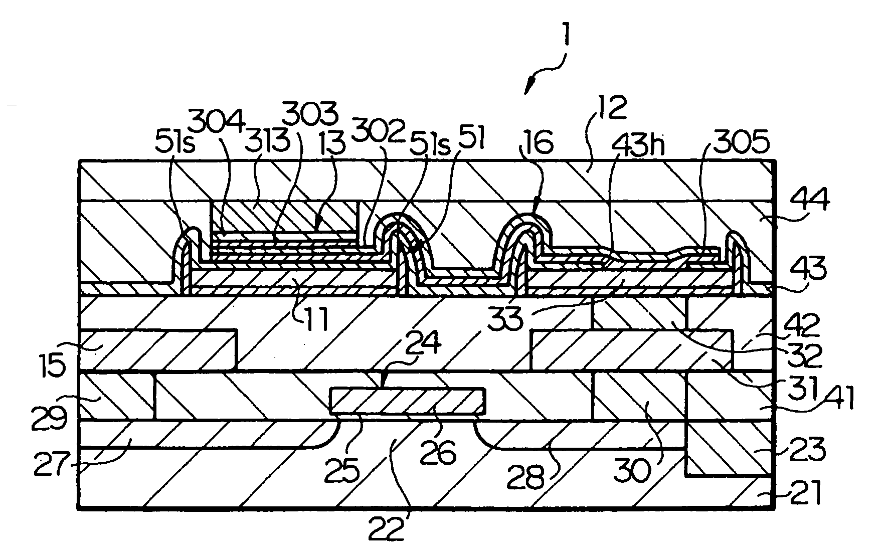
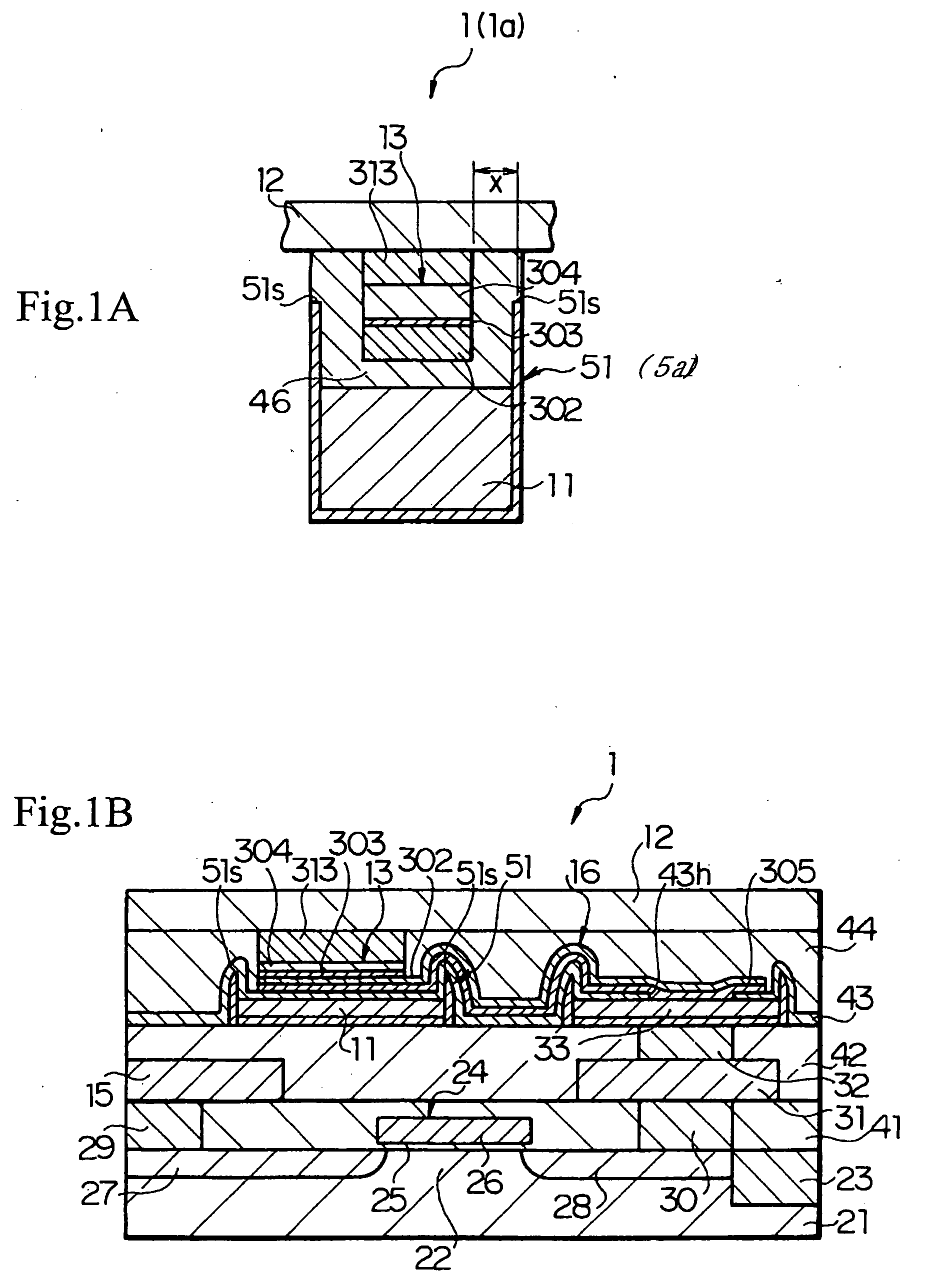
A magnetic memory device exhibits improved writing characteristics by providing a magnetic flux concentrator which efficiently applies the magnetic field, which is generated by the writing word line, to the memory layer of the TMR element. The magnetic memory device (1) is composed of the TMR element (13), the writing word line (the first wiring) (11) which is electrically insulated from the TMR element (13), and the bit line (the second wiring) (12) which is electrically connected to the TMR element (13) and intersecting three-dimensionally with the writing word line (11), with the TMR element (13) interposed therebetween. The magnetic memory device (1) is characterized as follows. The magnetic flux concentrator (51) of high-permeability layer is formed along at least the lateral sides of the writing word line (11) and the side of the writing word line (11) which is opposite to the side facing the TMR element (13). At least either of the side walls of the magnetic flux concentrator (51) projects from the writing word line (11) toward the TMR element (11).
Description
TECHNICAL FIELD [0001] The present invention relates to a magnetic memory device and a producing method thereof, and more particularly, to a non-volatile magnetic memory device and a producing method thereof. The magnetic memory device is designed to record information by utilizing the fact that the ferromagnetic body constituting the tunnel magnetoresistance element changes in resistance depending on whether the spin direction is parallel or anti-parallel. BACKGROUND ART [0002] The recent wide spread of information and communications equipment, particularly personal small ones such as portable terminals, requires their constituents (such as memory elements and logic elements) to have improved performance, including high integration, high speed, and low power consumption. Particularly, non-volatile memory is regarded as an indispensable element in the age of ubiquitous computing. [0003] Non-volatile memory preserves personal important information in case of dead battery and network ...
Claims
Login to View More Application Information
Patent Timeline
 IPC IPC(8): G11C11/15G11C11/16H01F10/16H01F10/30H01F10/32H01L21/8246H01L27/105H01L27/22H01L29/68H01L29/82H01L43/08
CPCG11C11/16H01L27/224H01L27/228H01L43/08H01L2924/0002H01L2924/00G11C11/1657G11C11/1675G11C11/1655H10B61/10H10B61/22H10N50/10
Inventor MOTOYOSHI, MAKOTOIKARASHI, MINORU
Owner SONY CORP