Semiconductor laser device, and method of manufacturing the same

a laser device and semiconductor technology, applied in the direction of lasers, semiconductor lasers, active medium materials, etc., can solve the problems of device characteristics, device characteristics vary, device characteristics degrade, etc., and achieve excellent controllability of transverse mode, and satisfactory difference of refractive index

Inactive Publication Date: 2005-08-04
NICHIA CORP
View PDF8 Cites 38 Cited by
  • Summary
  • Abstract
  • Description
  • Claims
  • Application Information

AI Technical Summary

Benefits of technology

[0016] In the first semiconductor laser device of the present invention constituted as described above, since the waveguide region has the first waveguide region where light is confined within the active layer by actually providing a difference in the refractive index between the active layer and the regions on both sides of the active layer, oscillation in the transverse mode can be more surely suppressed in the first waveguide region and the beam can be controlled reliably thereby emitting laser beam having excellent F.F.P.
[0041] In the second and third semiconductor laser devices, width of the stripe ridge is preferably in a range from 1 μm to 3 μm. With this constitution, the stripe waveguide region of excellent controllability of the transverse mode can be formed within the waveguide layer in the first waveguide region C1 and the second waveguide region C2, thus achieving a laser device free of kink in the current optical output characteristic.

Problems solved by technology

In the case of a semiconductor laser device made from a semiconductor material which is likely to suffer significant etching damage in the active layer or damage caused by exposing the active layer surface to the etching atmosphere, laser characteristics degrade due to the etching damage in the active layer and on the active layer surface when a semiconductor laser device of perfect refractive index guided type is made by etching deeper than the active layer thereby forming ridges.
However, in the case of effective refractive index type waveguide structure, variations in the device characteristics due to the variation in the stripe configuration mentioned above become significant, thus resulting in considerable variations in the device characteristics during volume production.
However, the structure of the laser devices known at present has a bottle neck in the formation of the ridge waveguide.
That is, since the transverse mode is controlled by the configuration, particularly height and width, of the ridge that constitutes the ridge waveguide and the far field pattern (F.F.P.) of the laser beam is determined accordingly, an error in the control of the depth of etching when forming the ridge waveguide is a major factor which directly causes variations in the device characteristics.
Dry etching techniques such as reactive ion etching (RIE) have been known for etching nitride semiconductor, but it has been difficult to control the depth of etching to such an accuracy as to completely solve the problem of variations in the device characteristics with these etching techniques.
Specifically, when forming the layers which constitute the device structure, the layers are formed with an extremely high accuracy and it is difficult to achieve the device structure of sophisticated design by forming the ridge and other structure with the etching technique having an accuracy lower than the accuracy of film forming by several orders of magnitude, thus making an obstacle to the improvement of device characteristics.
When the RIE process is employed for etching the nitride semiconductor, the layer exposed by etching and the surface thereof are prone to damage, which leads to deterioration of the device characteristics and reliability.

Method used


Image

  • Semiconductor laser device, and method of manufacturing the same
  • Semiconductor laser device, and method of manufacturing the same
  • Semiconductor laser device, and method of manufacturing the same

Examples


embodiment 1

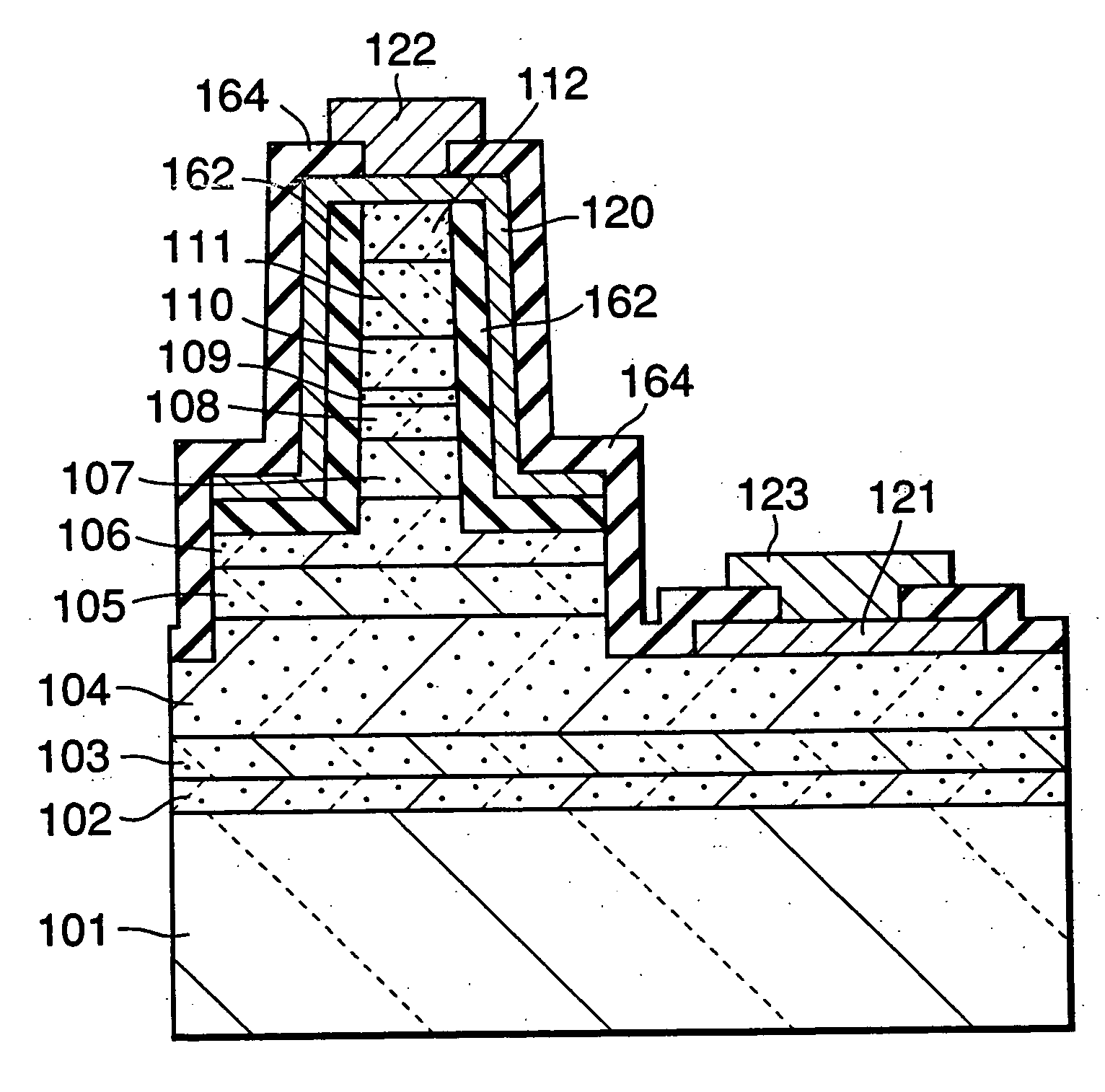
[0166] A laser device of the first embodiment will be described below. Specifically, the laser device comprising the second waveguide region C2 which has the sectional structure shown in FIG. 8 and the first waveguide region C1 which has the sectional structure shown in FIG. 9 is made as the first embodiment.

[0167] While a substrate made of sapphire, namely a material different from the nitride semiconductor is used in the first embodiment, a substrate made of nitride semiconductor such as GaN substrate may also be used. As the substrate of different material, an insulating substrate such as sapphire and spinel (MgAl2O4) each having the principal plane in either the C plane, R plane or A plane, SiC (including 6H, 4H and 3C), ZnS, ZnO, GaAs, Si, or an oxide which can be lattice matched with the nitride semiconductor can be used as long as the nitride semiconductor can be grown on the substrate. As the substrate of different material, sapphire and spinel are preferably used. The subs...

embodiment 2

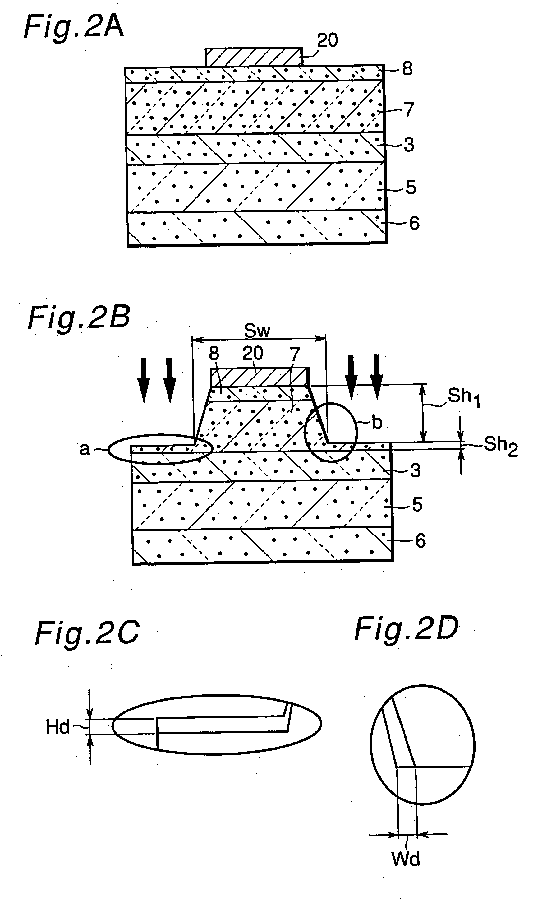
[0199] The laser device is fabricated similarly to the first embodiment except for the length of the first waveguide region C1 which is set to 1 μm. In order to form the first waveguide region C1 with such a small length, the first ridge of stripe shape is formed longer than the final length of the resonator (for example, several tens to about 100 μm) and then the resonance end face is formed by etching or dividing, the substrate at such a position as the desired length of the first waveguide region C1 is obtained. As a result, it becomes more difficult to form the second ridge 201 with stable shape than in the case of the first embodiment, although the transverse oscillation mode can be well controlled even with this length. Also shorter length of the first waveguide region improves the device life slightly over the first embodiment.

embodiment 3

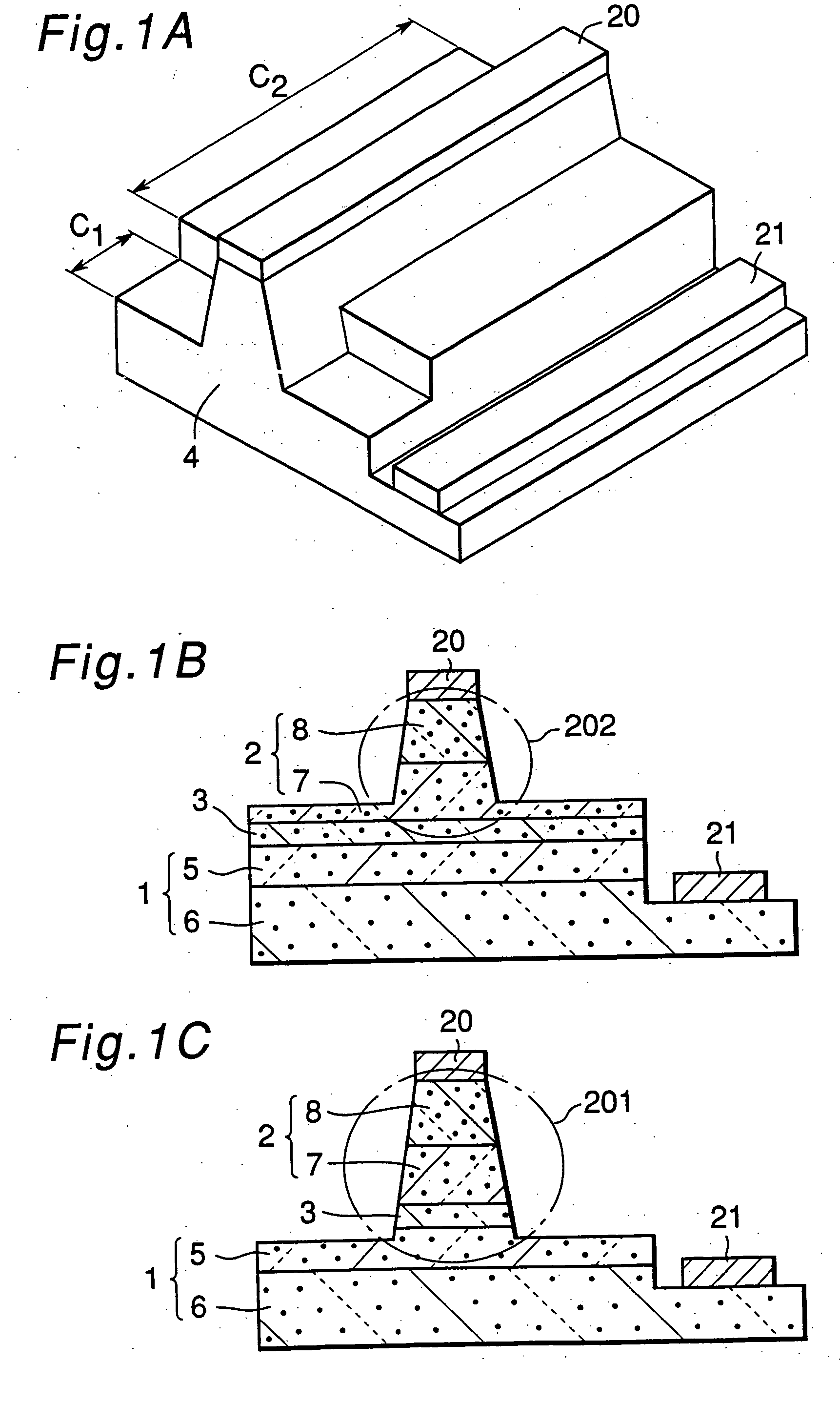
[0200] The laser device of the third embodiment is constituted similarly to the first embodiment except for forming the first waveguide regions C1 having length of 5 μm at both ends thereof (refer to FIG. 4B). That is, the laser device of the third embodiment has the second waveguide region C2 located at the center and the first waveguide regions C1 located on both sides of the former, while the first waveguide region C1 includes the resonator end face. The laser device of the third embodiment having such a constitution has both F.F.P. and aspect ration of the beam similar to those of the first embodiment.


PUM


Abstract

A semiconductor laser device comprises a laminate consisting of a semiconductor layer of first conductivity type, an active layer and a semiconductor layer of second conductivity type, which is different from the first conductivity type, that are stacked in order, with a waveguide region being formed to guide a light beam in a direction perpendicular to the direction of width by restricting the light from spreading in the direction of width in the active layer and in the proximity thereof, wherein the waveguide region has a first waveguide region and a second waveguide region, the first waveguide region is a region where light is confined within the limited active layer by means of a difference in the refractive index between the active layer and the regions on both sides of the active layer by limiting the width of the active layer, and the second waveguide region is a region where the light is confined therein by providing effective difference in refractive index in the active layer.

Description

BACKGROUND OF THE INVENTION [0001] The present invention relates to a semiconductor laser device having stripe ridge being formed. More particularly, the present invention relates to a semiconductor laser device which uses GaN, AlN or InN, or the Group III-V nitride compound semiconductor (InbAldGa1-b-dN, 0≦b, 0≦d, b+d<1) that is a mixed crystal of the compounds described above. [0002] Description of Related Arts [0003] Recently, nitride semiconductor laser devices have been receiving increasingly demands for the applications in optical disk systems such as DVD which are capable of recording, and reproducing a large amount of information with a high density. Accordingly, vigorous research efforts are being made in the field of nitride semiconductor laser device. Because of the capability to oscillate and emit visible light over a broad spectrum ranging from ultraviolet to red, the nitride semiconductor laser device is expected to have wide applications such as light sources for l...

Claims


Application Information

Patent Timeline
Patent Type & Authority Applications(United States)
IPC IPC(8): H01S5/10H01S5/20H01S5/22H01S5/227H01S5/323
CPCH01S5/0655H01S5/1014H01S5/1064H01S5/20H01S2301/18H01S5/22H01S5/227H01S5/2275H01S5/32341H01S5/2004
Inventor MATSUMURA, HIROAKI
Owner NICHIA CORP
Why Eureka
Try Eureka