Method and apparatus for high-speed thickness mapping of patterned thin films
- Summary
- Abstract
- Description
- Claims
- Application Information
AI Technical Summary
Benefits of technology
Problems solved by technology
Method used
Image
Examples
first embodiment
A First Embodiment
System for Measurements at an Angle
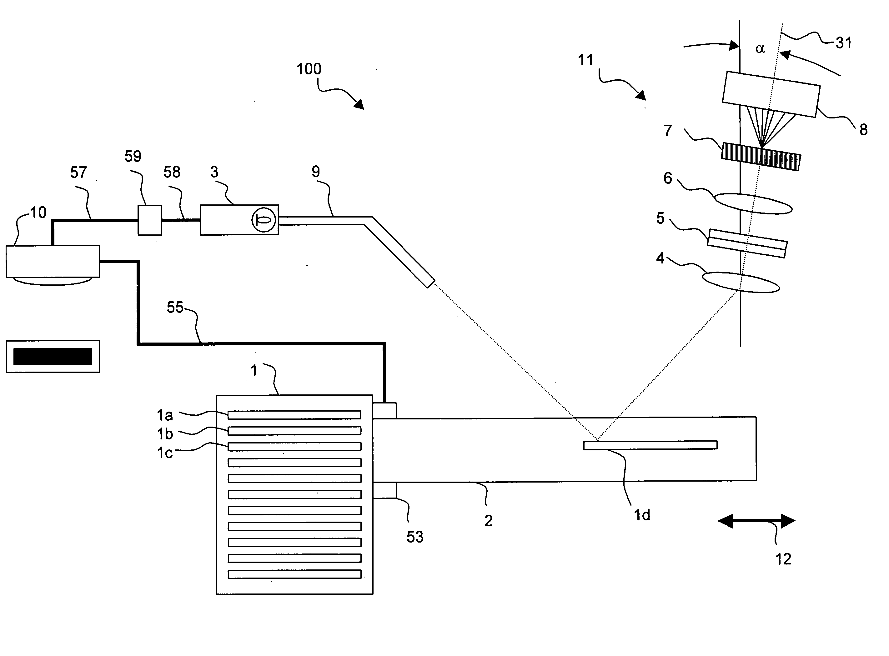
[0061] A first embodiment of an imaging system 100 in accordance with the subject invention, suitable for use in applications such as measuring the thickness of transparent or semi-transparent films, is illustrated in FIG. 1. Advantageously, the film to be measured ranges in thickness from 0.001 μm to 50 μm, but it should be appreciated that this range is provided by way of example only, and not by way of limitation. This embodiment is advantageously configured for use with a wafer transfer station 1 to facilitate rapid measurement of a cassette of wafers. The station houses a plurality of individual wafers 1a, 1b, 1c, and is configured to place a selected one of these wafers, identified with numeral 1d in the figure, onto a platform 2. Each of wafers 1a, 1b, 1c, and 1d has a center point and an edge. This embodiment also comprises a light source 3 coupled to an optical fiber 9 or fiber bundle for delivering light from the light ...
commercial embodiment
[0087] A commercial embodiment of a system according to the invention will now be described. The manufacturers of the components of this system are as identified in the previous example, with the exception of the lens assembly used in the spectrometer. In lieu of standard lenses designed for use with 35 mm cameras, this embodiment employs high quality lenses and mirrors manufactured by Optics 1 of Thousand Oaks, Calif. These lenses and mirrors are such that the modulation transfer function (MTF) for a plurality of alternating black and white line pairs having a density of about 40 line pairs / nun is greater than 70% over the entire wavelength range of interest.
[0088] This system is configured to measure the thicknesses of individual layers of a sample, e.g., a patterned semiconductor wafer, at desired measurement locations. The coordinates of these desired measurement locations are provided to the system. Rather than rely on complicated and unreliable traditional pattern recognition...
embodiment
Method of Operation—Commercial Embodiment
[0113]FIG. 11 is a flowchart of the method of operation followed by the current commercial embodiment for each layer in the sample being evaluated. The sample may be a semiconductor wafer or some other sample. In step 1100, the reflectance spectra for a plurality of spatial locations on the surface of a sample are simultaneously captured. The spatial locations may be in the form of a line, or some other shape, such as a curved shape, although in the current commercial embodiment, the locations are in the form of a line.
[0114] In step 1004, an evaluation is made whether all or a substantial portion of the entire surface has been scanned. If not, step 1102 is performed. In step 1102, a relative translation is performed between the surface of the sample and the light source and sensor used to perform the capture process. Again, this step can occur by moving the surface relative to one or the other of the light source and sensor, or vice-versa. ...
PUM
 Abstract
Description
Claims
Application Information


