Rectangular contact lithography for circuit performance improvement and manufacture cost reduction

a technology of rectifying contact lithography and circuit design, applied in the field of optical lithography, can solve the problems of inability to enforce the physical design constraints of strong-rets imposed on circuit design, the halting of the improvement of optical lithography equipment, and the inability to implement in the past, so as to achieve the effect of minimizing extra costs

Active Publication Date: 2005-09-08
THE UNIVERSITY OF HONG KONG
View PDF0 Cites 176 Cited by
  • Summary
  • Abstract
  • Description
  • Claims
  • Application Information

AI Technical Summary

Benefits of technology

[0013] Accordingly, it is an object of the present invention to provide a lithography method by which circuit area and performance of standard cells in application-specific integrated circuits (ASICs) is improved while manufacturing cost is reduced.
[0015] It is yet another object of the present invention to provide a lithography method by introducing less extra restrictions in layout design when apply fabrication-friendly contacts on design of standard cells in application-specific integrated circuits (ASICs).
[0018] A reusable chromeless alternating phase-shifting template mask is exposed first. The opposite phase shift of periodic 0° and 180° regions on the chromeless phase-shifting template mask creates periodic unexposed dark lines at the boundary of 0° and 180° regions. The period of the 0° and 180° regions on the chromeless alternating phase-shifting template mask is design to be one transistor pitch so that the period of the dark lines is half of that. The exposure of a contact trim mask on these periodic dark lines removes the unwanted parts of the dark lines and the small cuts of the dark lines left form the regularly-placed contacts.
[0021] A regular placement of contacts enables more effective use of resolution enhancement technologies, which in turn allows a reduction of manufacturing cost and the minimum contact size and pitch. However, the extra restrictions in layout increase the complexity of a layout design and might offset the benefits from the reduced contact size and pitch. Whether a circuit area will be smaller or not after using a regular contact placement depends on applications. It should be studied extensively to seek a fine balance between design flexibility and manufacturability.
[0024] A reusable chromeless alternating phase-shifting template mask is exposed first. The opposite phase shift of periodic 0° and 180° regions on the chromeless phase-shifting template mask creates periodic unexposed dark lines at the boundary of 0° and 180° regions. The period of the 0° and 180° regions on the chromeless alternating phase-shifting template mask is design to be one transistor pitch so that the period of the dark lines is half of that. The exposure of a contact trim mask on these periodic dark lines remove the unwanted parts of the dark lines and the small cuts of the dark lines left form the rectangular-placed contacts.
[0026] There are 2 masks (1 reusable template mask and 1 application-specific trim mask) and 2 exposures are needed to fabricate the rectangular regularly-placed contacts in standard cell. Since there is no extra application-specific mask needed comparing with the conventional lithography method for unrestrictedly-placed contacts, extra cost is minimized

Problems solved by technology

However, the improvement of optical lithography equipment come to a halt due to the extreme technology challenges in developing the next generation optical imaging system with a smaller illumination wavelength.
However, although the achieved resolution can be doubled, challenges associated with the two-beam imaging, not only for electronic design automation (EDA) solutions, but also for manufacturing cost, prevented it from being implemented in the past.
Physical design constraints required by strong-RETs imposed on circuit design and cannot be enforced through conventional design flows.
The RET-embedded design flow, which is required by the strong-RET-imposed layout restrictions to guarantee layout-compliant designs, is significantly more complicated than conventional flow and requires a design and process integration (DPI).
That increases difficulties in EDA software design and requires layout designers to have a good knowledge of the strong-RETs used in a process.
Furthermore, the process-specific nature of RET-specific optimization in the new flow does not ensure design compatibility with future lithography solutions.
All of these increase design cost for sub-100 nm technology nodes as well as manufacturing cost which has been pushing to an alarming level because of increasingly complicated fabrication process with highly-optimized RETs.
However, there is no “free lunch” in the world.
As a trade-off between design flexibility and manufacturability, fabrication-friendly layout decreases the flexibility in physical design.
Although the features can be designed smaller and packed closer, the excessive lithography friendliness in fabrication-friendly layout may be so restrictive on layout design that circuit area increases unacceptably.
Contact level is one of the most difficult parts of a lithography process and has the biggest cost weighting.
Applying a regular placement on the contacts in the height direction cannot help to decrease the height of a standard cell except for an increased difficulty in the layout compaction.
However, there are several difficulties to apply such a regularly-placed layout on a standard cell.
Although multiple exposures can be introduced to fabricate the new layout [SN96,WJ03], it increases the cost and decreases the throughput.

Method used


Image

  • Rectangular contact lithography for circuit performance improvement and manufacture cost reduction
  • Rectangular contact lithography for circuit performance improvement and manufacture cost reduction
  • Rectangular contact lithography for circuit performance improvement and manufacture cost reduction

Examples


Embodiment Construction

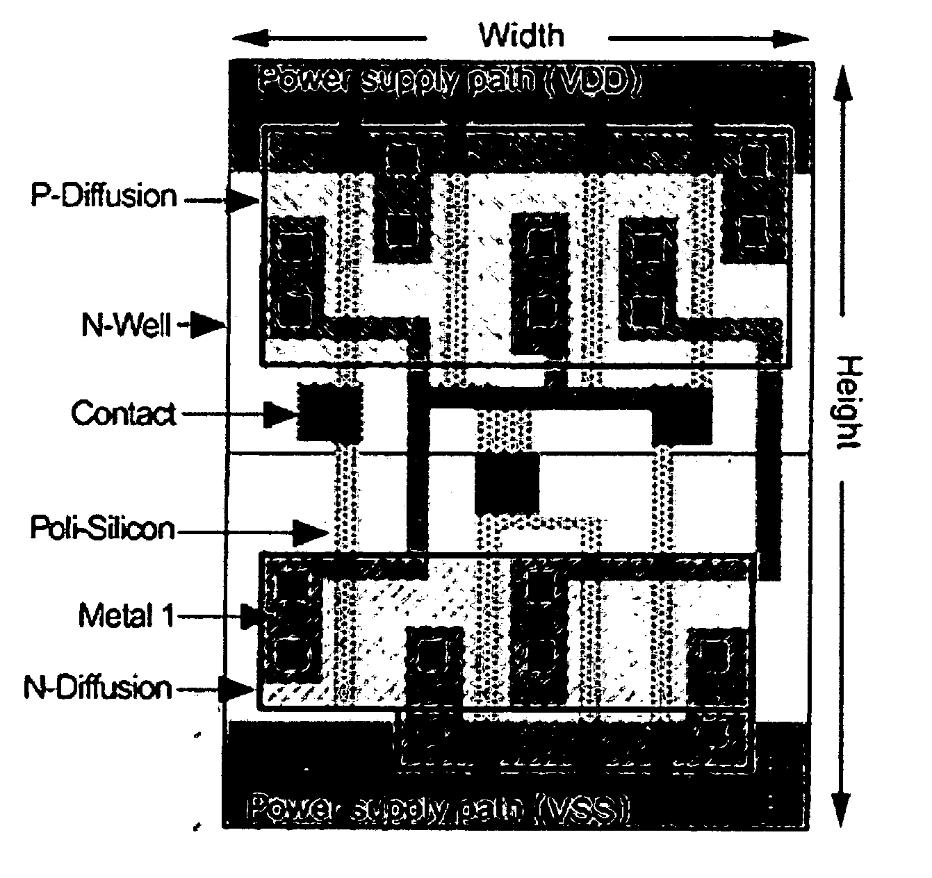
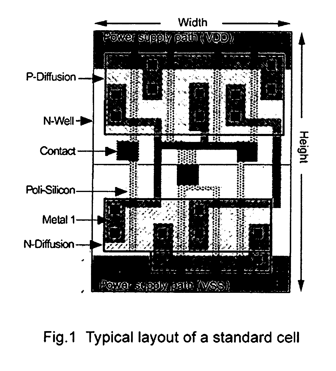
[0037]FIG. 1 is a diagram illustrating the structure of a standard cell. Each standard cell in a library is rectangular with a fixed height but varying widths. The cells are placed in rows with overlapping power supply paths. A standard cell typically has an N-well layer, an N-diffusion layer, a P-diffusion layer, a poly-silicon layer, a contact layer, and a metal-1 layer. The N-well, N-diffusion 330, P-diffusion and poly-silicon form P-MOS and N-MOS inside the cells. The poly-silicon also serves as an intra-cell routing path. The contacts 360 form connections between the routing layers and the under layers.

[0038] The height of a cell is typically given as the number of metal-1 tracks over the cells in the height direction. A metal-1 track comprises the metal-1 path and the space between metal-1 paths. The typical height of a standard cell is 10 tracks, where three tracks are used for power supply paths and the remaining seven tracks are for intra-cell design.

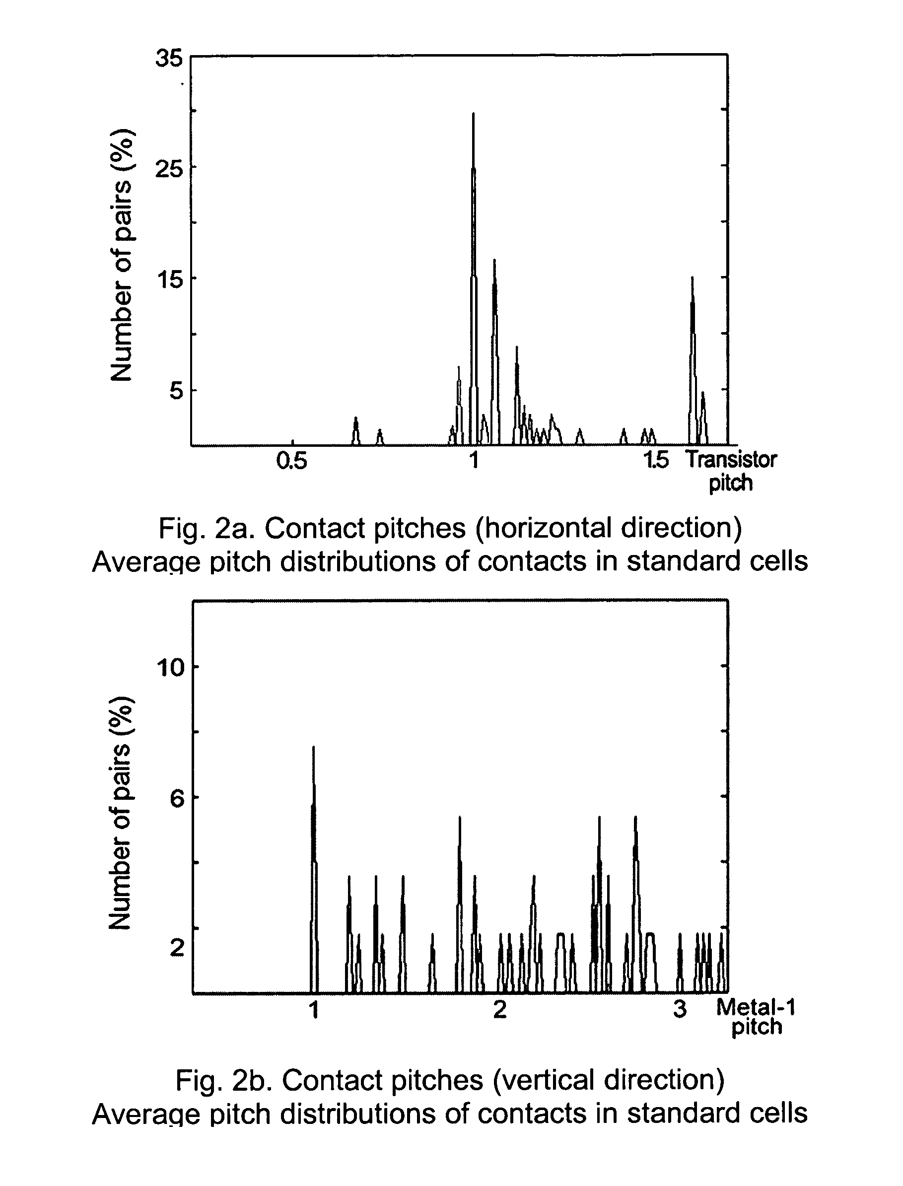
[0039] Placing featur...


PUM

PropertyMeasurementUnit
feature sizeaaaaaaaaaa
contact sizeaaaaaaaaaa
sizeaaaaaaaaaa

Abstract

An optical lithography method is disclosed that uses double exposure of a reusable template mask and a trim mask to fabricate regularly-placed rectangular contacts in standard cells of application-specific integrated circuits (ASICs). A first exposure of the reusable template mask with periodic patterns forms periodic dark lines on a wafer and a second exposure of an application-specific trim mask remove the unwanted part of the dark lines and the small cuts of the dark lines left form the rectangular regularly-placed contacts. All contacts are placed regularly in one direction while unrestrictedly in the perpendicular direction. The regular placement of patterns on the template mask enable more effective use of resolution enhancement technologies, which in turn allows a decrease in manufacturing cost and the minimum contact size and pitch. Since there is no extra application-specific mask needed comparing with the conventional lithography method for unrestrictedly-placed contacts, the extra cost is kept to the lowest. The method of the invention can be used in the fabrication of standard cells in application-specific integrated circuits (ASICs) to improve circuit performance and decrease circuit area and manufacturing cost.

Description

CROSS-REFERENCE TO RELATED APPLICATIONS [0001] This application is a non-provisional based on U.S. Provisional Application Ser. No. 60,546,948, filed Feb. 24, 2004, which is incorporated herein in its entirety by reference.FIELD OF THE INVENTION [0002] The present invention relates to optical lithography. More specifically, the invention relates to a double-exposure photolithography method using a reusable template mask and a trim mask to image regularly-placed rectangular contacts. The method of the invention can be used in the fabrication of a contact layer of standard cells in application-specific integrated circuits (ASICs) to improve circuit performance and decrease circuit area and manufacturing cost. BACKGROUND OF THE INVENTION [0003] The continuous demand for high speed integrated circuits (ICs) results in the continuous increase of transistor density and decrease of the feature size in the past two decades. As a technology to print circuit patterns with submicron features, ...

Claims


Application Information

Patent Timeline
Patent Type & Authority Applications(United States)
IPC IPC(8): G03F1/14G03F7/20G03F9/00H01L21/00
CPCG03F1/144G03F7/70466G03F7/70283G03F1/70
Inventor WANG, JUNWONG, ALFRED K.LAM, EDMUND Y.
Owner THE UNIVERSITY OF HONG KONG
Why Eureka
Try Eureka