Substrate, conductive substrate, fine structure substrate, organic field effect transistor and manufacturing method thereof

a technology of organic field effect transistor and conductive substrate, which is applied in the direction of sustainable manufacturing/processing, instruments, and final product manufacturing, etc., can solve the problems of difficult formation of fine patterns with a line width of 10 m or less, photolithography method requires a large number of steps, and the cost of photolithography method is high

Inactive Publication Date: 2005-09-15
CANON KK
View PDF14 Cites 59 Cited by
  • Summary
  • Abstract
  • Description
  • Claims
  • Application Information

AI Technical Summary

Benefits of technology

[0022] The present invention has been accomplished in view of the prior art, and it is, therefore, an object of the present invention to provide a substrate, an organic field effect transistor and a manufacturing method thereof in which a desired layer can be formed even on a base material having much unevenness or many protuberances on a surface thereof such as a resin base material.

Problems solved by technology

As described above, the photolithography method requires very large number of steps.
Therefore, the photolithography method is costly.
However, in the case of a printing method such as screen printing, for example, formation of a fine pattern with a line width of 10 μm or less entails difficulties.
On the other hand, such printable electrode material is becoming capable of obtaining a high conductivity similar to that of an evaporated metal film, which poses the large problem that a calcination temperature of 150° C. or more will be required in order to attain such a high conductivity.
Polyethylene terephthalate (PET) film, which is the most general-purpose resin base material at present, is inferior in terms of heat resistance and is therefore difficult to be used when heated, e.g., to 150° C. or more.
On the other hand, polyethylene naphthalate (PEN) and polyimide base materials withstand heating up to about 200° C. but is expensive compared with PET.
In addition, in the case of forming an electrode pattern using liquid through printing or the like, the surface state of the base material affects the characteristics of the obtained film, which results in the possibility that no desired conductivity may be obtained or necessitates that the film is made thicker than needed.
Although a resin base material formed in a seat shape has the advantages of high processability and deformability as well as inexpensiveness, a number of steps or unevennesses generated at the time of forming are recognizable and the surface flatness and smoothness are inferior to those of glass or silicon base material, which has been a problem.
In the case where a solution was coated on such resin base material surface with the aid of a bar coater and dipping, uniform coating has been difficult.
The film characteristics after the calcination have not also been uniform.
Moreover, also in case of using pastes to form a pattern, the pattern shape and the resolution is largely affected by the unevenness or wettability of the base material surface.
The former chemical treatment method is exemplified by a method of immersing a base material in sulfuric acid to make the surface hydrophilic, which, however, may cause a serious damage depending on the kind of the base material and necessitates post-treatment cleaning.
However, because the effect of surface modification by the treatment will vary depending on the kinds of base materials, the applicable base materials are limited, which has been a problem.
When a thick film is to be obtained or the fixing operation is omitted, there has been a possibility that swelling may occur at the time of the immersion in water (Japanese Patent Application Laid-Open No.
However, although the film formation of TiO2 is performed at ordinary temperature, long-time ultraviolet irradiation is required in order to decrease the water contact angle to lengthen the manufacturing time, so that much cost reduction cannot not be accomplished.
However, because in general a metal oxide cannot be formed into a film in a thickness of a micrometer order and the bumps of the resin substrate cannot therefore be filled, no resin substrate of good smoothness will not be obtained.
Moreover, the obtained pattern will suffer from blurring (staining), so that no fine pattern can be obtained.
In the case of the sol-gel process, in order to obtain an anatase-type crystal with good photosensitivity, a high-temperature calcination above 200° C. is required, giving rise to the above-mentioned problem of unemployability of PET or the like, accompanied by the problem that the available resin substrates are limited.
In this case, although the polymer compound can be grown at a low temperature, the resin substrate surface is rough, so that no fine pattern can be formed, which is a problem.
In general, a surface of an organic semiconductor material will be discomposed with UV light or the like, and therefore in the case of such stacking order, changing the surface energy by use of UV light may result in lowering in the performance.
In addition, because source and drain electrodes are formed on a substrate, an insulating film on the source and drain electrodes will be thin, thereby posing the problem that a leak current is apt to be generated.
As described above, in the case of forming layers such as electrodes on a general-purpose resin base material, the existence of unevenness on the base material has resulted in difficulty in forming a desired layer such as electrode with a low resistance and uniform characteristics by use of a dispersion liquid or paste of conductive fine particles.

Method used


Image

  • Substrate, conductive substrate, fine structure substrate, organic field effect transistor and manufacturing method thereof
  • Substrate, conductive substrate, fine structure substrate, organic field effect transistor and manufacturing method thereof
  • Substrate, conductive substrate, fine structure substrate, organic field effect transistor and manufacturing method thereof

Examples


example 1

[0274] The organic resin solution 1 was coated onto a PET film with a dip coater, and thereafter was heated in a hot-air circulating oven at 180° C. for an hour to form an organic resin layer with a film thickness of 3 μm.

[0275] No cracks and the like were observed on the formed organic resin layer surface with visual observation. The water contact angle of the substrate surface was 63°. In addition, the surface resistivity of the organic resin layer surface was measured with a high-resistivity measuring device (made by Mitsubishi Chemical Corporation, trade name Hiresta UP MC P-HT450 [probe URS]), and was 1×10¹³ Ω / □ or more at an applied voltage of 100 V. Moreover, the heat characteristic of the film obtained by heating the organic resin solution 1 was analyzed with differential scanning calorimeter, and no glass transition temperature (Tg) was observed at 180° C. or less.

[0276] The surface roughness of the obtained substrate was measured with a scanning probe microscope (made by...

example 2

[0280] With the exception that the organic resin solution 1 was replaced with the organic resin solution 2, the same procedure as in Example 1 was followed. On the surface of the formed organic resin layer with a film thickness of 2.8 μm, no cracks and the like were observed with visual observation, and the water contact angle and the surface resistivity at 100 V of the substrate surface were respectively 63° and not less than 1×10¹³ Ω / □. Moreover, Tg of the film obtained by heating the organic resin solution 2 was not observed at 180° C. or less.

[0281] As with Example 1, surface roughness of the obtained substrate was measured and the average surface roughness (Ra′) of the organic resin layer of this substrate was 0.3 nm and the maximum peak height was 3 nm.

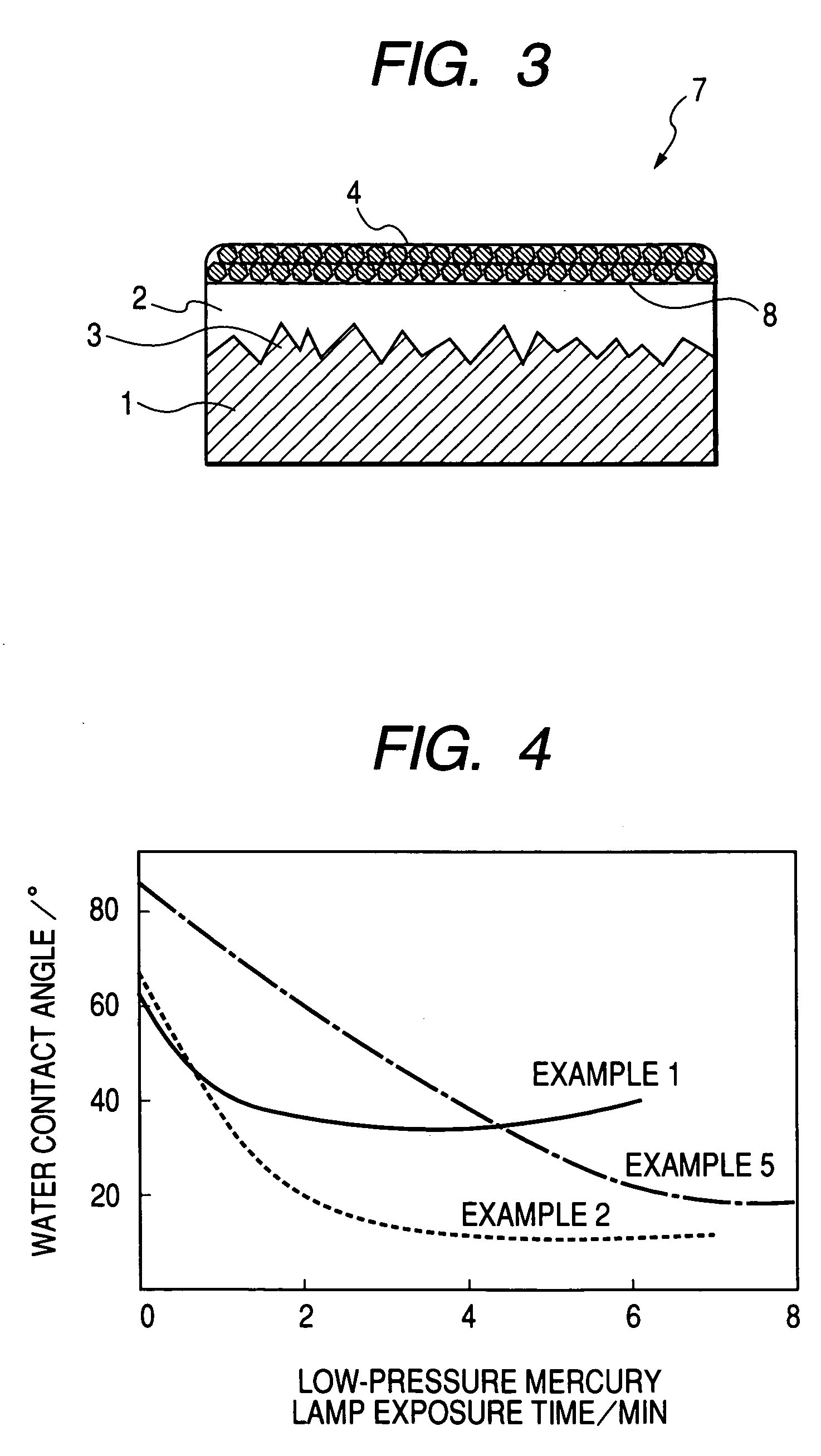
[0282] Subject to 3-minute exposure with a low-pressure mercury lamp, the water contact angle of the substrate surface, the average surface roughness and the maximum height were measured and were respectively 22°, 0.3 nm and 3...

example 3

[0283] With the exception that the organic resin solution 1 was replaced with the organic resin solution 3, the same procedure as in Example 1 was followed. On the surface of the formed organic resin layer with a film thickness of 3.6 μm, no cracks and the like were observed with visual observation, and the water contact angle and the surface resistivity at 100V both of the substrate surface were respectively 65° and not less than 1×10¹³ Ω / □. Moreover, Tg of the film obtained by heating the organic resin solution 3 was not observed at 180° C. or less.

[0284] As with Example 1, the surface roughness of the obtained substrate was measured and the average surface roughness (Ra′) of the organic resin layer of this substrate was 0.8 nm and the maximum peak height was 10 nm.

[0285] After 5-minute exposure with a low-pressure mercury lamp, the water contact angle of the substrate surface, the average surface roughness and the maximum height were measured and were respectively 20°, 0.8 nm a...


PUM

PropertyMeasurementUnit
heightaaaaaaaaaa
heightaaaaaaaaaa
heightaaaaaaaaaa

Abstract

A substrate is provided which comprises an organic resin layer on a base material, wherein the base material has an average surface roughness of not less than 1.2 nm but no more than 5 nm and a maximum height of a surface unevenness of not less than 0.1 μm but no more than 1.0 μm; the organic resin layer has an average surface roughness of not more than 1 nm and a maximum peak height of a surface unevenness of not more than 30 nm; and at least a part of a surface of the organic resin layer comprises a hydrophilic region.

Description

BACKGROUND OF THE INVENTION [0001] 1. Field of the Invention [0002] The present invention relates to a substrate, a conductive substrate, a fine structure substrate, an organic field effect transistor and a method of manufacturing them, in particular to a substrate, a conductive substrate and a method of manufacturing them in which variously applicable layers such as electrodes, metal wiring, insulating layers, and fine patterns of these layers can be formed on a base material having an unevenness such as resin material and in particular to a substrate, a conductive substrate, a fine structure substrate, an organic field effect transistor, and a method of manufacturing them in which a flat and smooth layer can be provided by a simple method such as coating on an inexpensive base material to form layers such as electrodes, metal wiring and an insulating layer easily with good adhesion and which can be used for making fine elements such as semiconductor elements, integrated circuits, ...

Claims


Application Information

Patent Timeline
Patent Type & Authority Applications(United States)
IPC IPC(8): B05D3/06B05D1/38B32B27/00G03F7/00H01L21/336H01L29/786H01L51/00H01L51/05
CPCH01L51/0022H01L51/0036Y02E10/549H01L51/052H01L51/0545H01L51/0096Y02P70/50H10K71/611H10K85/113H10K77/10H10K10/471H10K10/466
Inventor NAKAYAMA, TOMONARIOHNISHI, TOSHINOBUKUBOTA, MAKOTOMIURA, DAISUKE
Owner CANON KK
Why Eureka
Try Eureka