Waveguide compositions and waveguides formed therefrom
- Summary
- Abstract
- Description
- Claims
- Application Information
AI Technical Summary
Benefits of technology
Problems solved by technology
Method used
Image
Examples
example 1
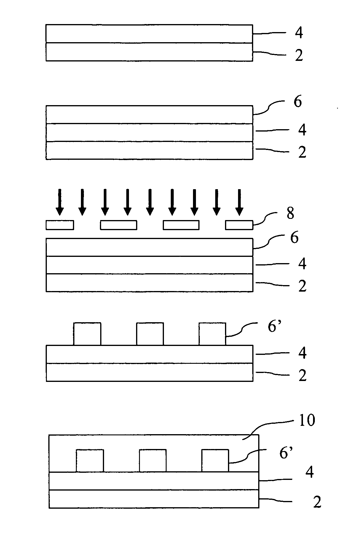
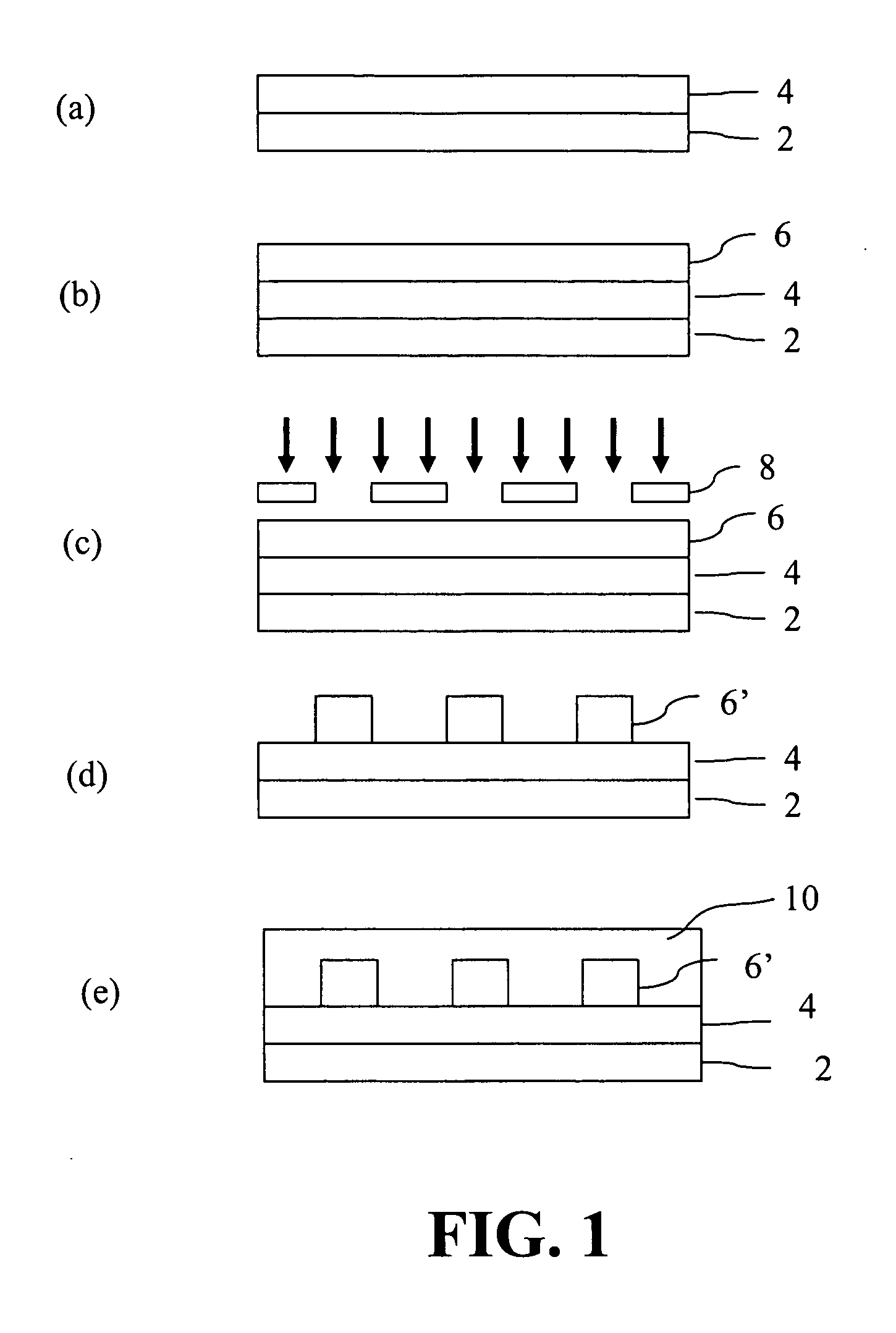
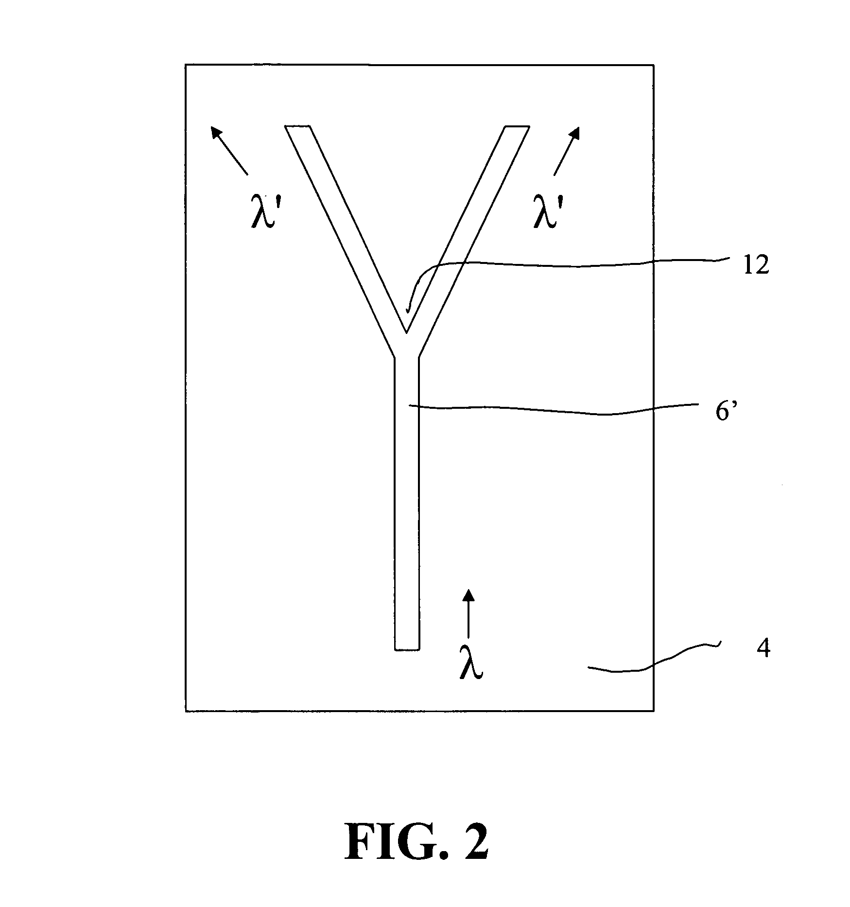
[0064] 45.76 wt % propylene glycol monomethyl ether acetate, 48.17 wt % phenyl-methyl-dimethyl silsesquioxane (49:49:2 wt % based on polymer), 1.1 wt % of epoxidized polybutadiene, 0.11 wt % hydroxy terminated diphenylnaphthylsulphonium perfluorobutanesulfonate, 4.82 wt % polydiphenylsiloxane and 0.007 wt % Dow SILWET L-7604 silicone-base oil were combined in admixture. The composition was coated onto pumice scrubbed copper foil using a #80 drawdown bar and dried in an oven for 15 minutes at 90° C. Artwork defining the required waveguide was placed directly on the composition. The artwork included patterns for forming waveguides of various dimensions and shapes, such as linear, branched, and curved shaped waveguides between 2 and 14 cm in length and 5 to 15 μm in width. 300 mJ / cm2 of actinic radiation was applied to the construction followed by a post-exposure-bake in air at 90° C. for 15 minutes. The exposed wafer was dipped in a 0.85N sodium hydroxide developer solution held at 37...
example 2
[0065] 45 wt % propylene glycol monomethyl ether acetate, 35 wt % of trifluoromethyl-phenyl-silsesquioxane (10:90 wt % based on polymer), 15 wt % 3,3-dimethyloxetane, 4.95 wt % benzoin tosylate, and 0.05 wt % Dow SILWET L-7604 silicone-base oil are combined in admixture. The composition is spin-coated at 2500 rpm onto a six-inch silicon dioxide-coated silicon wafer and soft-baked in air on a hot plate for two minutes at 90° C., to a thickness of 8 μm. Artwork as described in Example 1 is placed directly on the composition. 2000 mJ / cm2 of actinic radiation is applied to the construction followed by a post-exposure-bake in air at 90° C. for two minutes. The exposed wafer is then dipped in a propylene glycol monomethyl ether acetate developer solution held at 37.8° C. (100° F.) for 30 seconds. The wafer is then rinsed in de-ionized water and dried. The wafer is heated to 200° C. in air for 10 minutes on a hot plate. Flexible optical waveguides are expected to result.
example 3
[0066] 37 wt % propylene glycol monomethyl ether acetate, 47.99 wt % methyl-phenyl silsesquioxane (50:50 wt % based on polymer), 10 wt %, trimethylolpropane trivinyl ether, 5 wt % triphenylsulfonium trifluoromethylsulphonate, and 0.01 wt % Dow SILWET L-7604 silicone-base oil are combined in admixture. The composition is roller-coated onto 24 inch×36 inch (61 cm×91.4 cm) epoxy laminate, such as is commonly used in printed wiring board manufacture, to a thickness of 60 μm. The composition is then dried in air in a convection oven for 45 minutes at 90° C. Artwork as described in Example 1, but with line widths of 40 to 200 μm, is placed directly on the composition. 1000 mJ / cm2 of actinic radiation is applied to the construction, followed by a post-exposure-bake in air at 90° C. for 30 minutes. The exposed structure is then placed into a spray developer containing 0.7N sodium hydroxide developer solution held at 37.8° C. (100° F.) for a total of 120 seconds. The laminate is rinsed in de...
PUM
| Property | Measurement | Unit |
|---|---|---|
| Composition | aaaaa | aaaaa |
| Solubility (mass) | aaaaa | aaaaa |
| Flexibility | aaaaa | aaaaa |
Abstract
Description
Claims
Application Information


