
Method for improving electrical conductivity of metals, metal alloys and metal oxides

a technology applied in the field of metal alloys and metal oxides, can solve the problems of high cost of fabricating electrical devices incorporating these materials, high cost of materials employed, and time-consuming steps required to plate the substrate, so as to improve the quality of the treated surface, prevent substrate degradation and deformation, and enhance the electrical conductivity of metals

Inactive Publication Date: 2005-12-01
WILSON GREATBATCH LTD
View PDF12 Cites 5 Cited by
  • Summary
  • Abstract
  • Description
  • Claims
  • Application Information

AI Technical Summary

Benefits of technology

[0005] It would therefore, be highly desirable to provide a new and improved method for enhancing the electrical conductivity of metals, metal alloys and metal oxides which does not require additional heat treatment, which provides control over the density and depth of the material introduced to the treated surface, which can be performed in a manner preventing substrate degradation and deformation, and which improves the quality of the treated surface.
[0006] The present invention provides a method for improving the electrical conductivity of a substrate of metal, metal alloy or metal oxide which includes depositing a small or minor amount of metal or metals from Group VIIIA metals (Fe, Ru, Os, Co, Rh, Ir, Ni, Pd, Pt) or from Group IA metals (Cu, Ag, Au) on a substrate of metal, metal alloys and / or metal oxide from Group IVA metals (Ti, Zr, Hf), Group VA metals (V, Nb, Ta), Group VIA metals (Cr, Mo, W) and Al, Mn, Ni and Cu. The native oxide layer is changed from electrically insulating to electrically conductive. The depositing process is a low temperature arc vapor deposition process. This may be done in a deposition chamber. The deposition may be performed on either treated or untreated substrate. After deposition the substrate is available for use as a substrate and no other processing steps may be necessary.
[0007] The method of the present invention advantageously does not require additional heat treatment and provides control over the density and depth of the material introduced onto the treated surface thereby not affecting the bulk of the material. The method can be performed at a temperature sufficiently low so as to prevent substrate degradation and deformation. It is believed that the quality of the treated surface is improved by the method of the present invention. Multiple processing steps may be incorporated into the method, for example substrate cleaning, oxide removal and etching. Another advantage is that using a substrate treated by the method of the present invention will allow the surface thereof to be treated to passivate it from chemical reaction while still providing adequate electrical conductivity. Stainless steels having native insulating oxide layers also can be treated by the method of the present invention to provide an electrically conductive oxide layer.

Problems solved by technology

Such measures require special apparatus and extremely careful handling of the materials, all of which adds cost to the fabricating of electrical devices incorporating these materials to which electrical contact must be made.
The materials employed are expensive and the steps required to plate the substrate are costly and time consuming.
This, in turn, adds to the cost and complexity of the manufacturing process.

Method used


Image

  • Method for improving electrical conductivity of metals, metal alloys and metal oxides
  • Method for improving electrical conductivity of metals, metal alloys and metal oxides
  • Method for improving electrical conductivity of metals, metal alloys and metal oxides

Examples


example

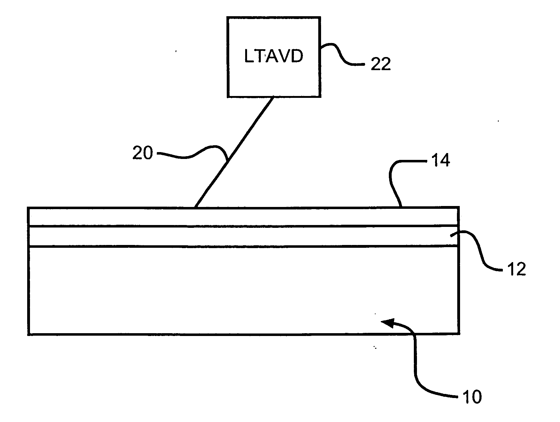
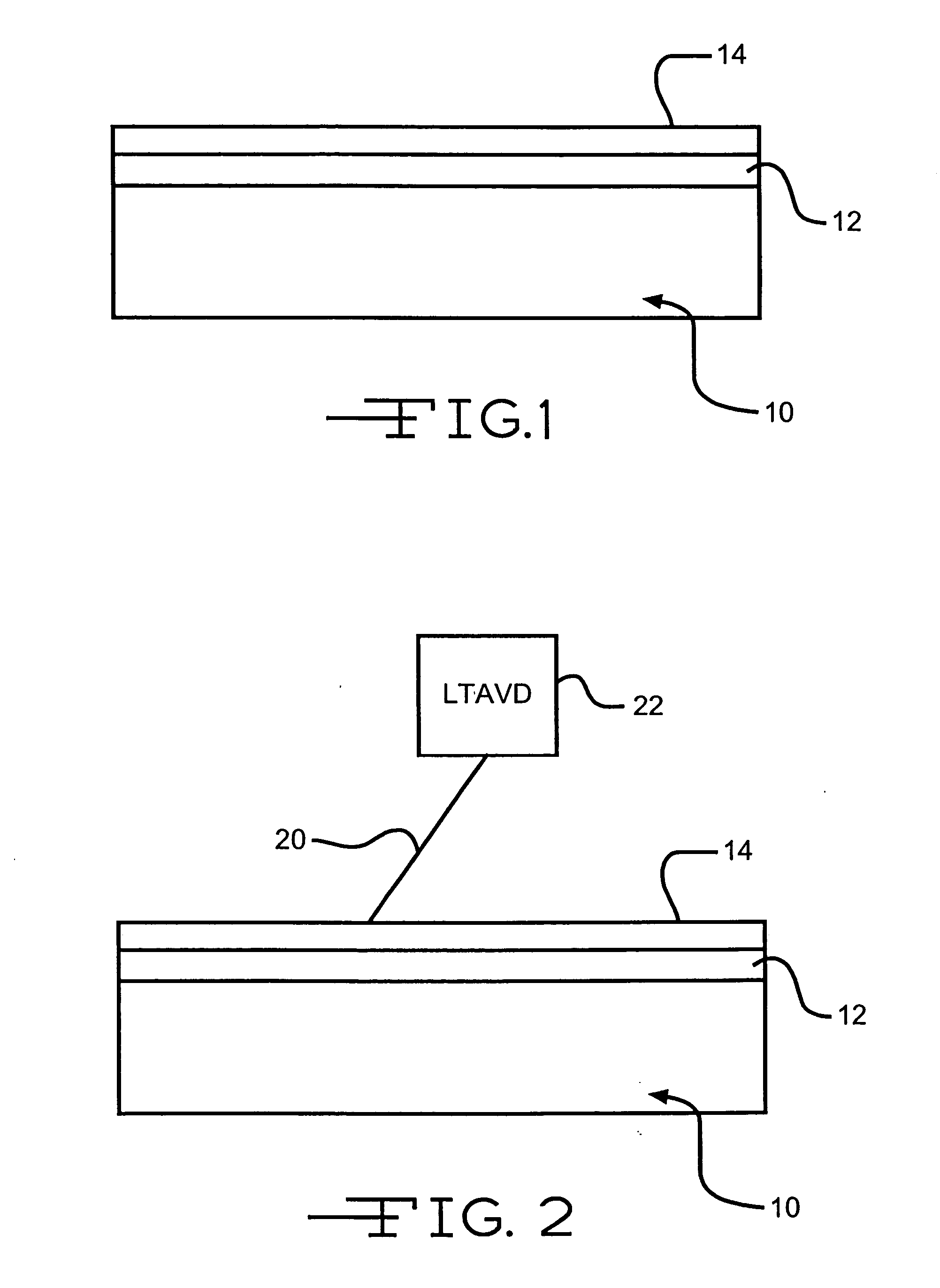
[0020] A tantalum or titanium substrate similar to substrate 10 shown in FIG. 1 is first abraded on one side using a 3M Scotch-brite pad of very fine type. This produces a rough surface on the side to be coated. It is then degreased and cleaned. This is accomplished by cleaning the foil in an ultrasonic bath using acetone as a solvent for 10 minutes. Next it is washed in an ultrasonic methanol bath and then blow dried using dry, clean compressed air.

[0021] The substrate is now ready to be coated with palladium. It is placed in a Low Temperature Arc Vapor Deposition (LTAVD) apparatus similar to apparatus 22 of FIG. 2 to be coated. After the sample is loaded into the apparatus the pressue in the deposition chamber is lowered by a vacuum pump to 10−5-10−6 Torr. This gets rid of all waste gases, specially oxygen. In this process oxygen is a contaminant. The pressue is brought up to the mTorr range by introducing argon into the chamber. The substrate is biased to 600V and an arc is stru...


PUM

PropertyMeasurementUnit
Thicknessaaaaaaaaaa
Temperatureaaaaaaaaaa
Timeaaaaaaaaaa

Abstract

A method for improving the electrical conductivity of a substrate of metal, metal alloy or metal oxide comprising depositing a small or minor amount of metal or metals from Group VIIIA metals (Fe, Ru, Os, Co, Rh, Ir, Ni, Pd, Pt) or from Group IA metals (Cu, Ag, Au) on a substrate of metal, metal alloys and / or metal oxide from Group IVA metals (Ti, Zr, Hf), Group VA metals (V, Nb, Ta), Group VIA metals (Cr, Mo, W) and Al, Mn, Ni and Cu. The native oxide layer of the substrate is changed from electrically insulating to electrically conductive. The step of depositing is carried out by a low temperature arc vapor deposition process. The deposition may be performed on either treated or untreated substrate. The substrate with native oxide layer made electrically conductive is useable in the manufacture of electrodes for devices such as capacitors and batteries.

Description

BACKGROUND OF THE INVENTION [0001] This invention relates to the art of treating metals, metal alloys and metal oxides, and more particularly to a new and improved method for enhancing the electrical conductivity of metals, metal alloys and metal oxides. [0002] One area of use of the present invention is in the manufacturing of electrodes for capacitors, batteries and the like, although the principles of the present invention can be variously applied. Metals and metal alloys have a native oxide present on the surface. This is an insulating layer and hence if the material is to be used as a substrate for an electrode, the oxide has to be removed or made electrically conductive. [0003] If the oxide is removed by chemical treatment, such as by etching with an acid or electrolytic etching to expose the underlying metal, special steps must be taken in order to complete the electrical contacts before the native oxide can be regenerated and interfere with the electrical contacts. Such meas...

Claims


Application Information

Patent Timeline
IPC IPC(8): B32B15/01C23C14/06C23C14/14C23C14/24C23C14/32
CPCC23C14/14C23C14/16C23C14/325Y10T428/12493C23C14/022Y10T428/12722Y10T428/12507B32B15/01
Inventor MUFFOLETTO, BARRYSHAH, ASHISH
Owner WILSON GREATBATCH LTD
Learn More