Semiconductor integrated circuit device having improved punch-through resistance and production method thereof, semiconductor integrated circuit device including a low-voltage transistor and a high-voltage transistor

a technology of integrated circuit device and punch-through resistance, which is applied in the direction of semiconductor integrated circuit device including low-voltage transistor and high-voltage transistor, can solve the problems of increased fabrication cost, limited degree of freedom of process, and large difference in device structure and operation voltage between flash memory device and logic device, so as to increase the threshold voltage of parasitic field transistor and boost the voltage efficiently. , the effect of high resistan

Inactive Publication Date: 2005-12-22
FUJITSU SEMICON LTD
View PDF8 Cites 108 Cited by
  • Summary
  • Abstract
  • Description
  • Claims
  • Application Information

AI Technical Summary

Benefits of technology

[0140] According to the present invention, the conductor pattern formed on the second device isolation insulation film is formed of a polysilicon layer of low impurity concentration level and a metal silicide layer formed thereon, and thus, there is caused depletion in the polysilicon layer in the case a voltage is applied to the metal silicide layer, and conduction of the parasitic field transistor having a channel right underneath the device isolation insulation film is suppressed effectively, even in the case the thickness of the second device isolation insulation film constituting the second the device isolation structure is reduced. With regard to the conductor pattern, on the other hand, a polysilicon film of high resistance such as a polysilicon film of low impurity concentration level or undoped polysilicon film free form impurity element is used, wherein there arises no problem of increase of resistance for the conductor pattern, as there is formed a low resistance metal silicide layer on the surface of such a polysilicon film. With this, it becomes possible to increase the threshold voltage of the parasitic field transistor while suppressing increase of the substrate impurity concentration level, which may cause increase of threshold voltage of the high voltage transistor.
[0141] Another object of the present invention is to provide a semiconductor integrated circuit device in which a non-volatile semiconductor device and a logic device are integrated on a substrate together with a boosting element cable of boosting a voltage efficiently even in the case a low voltage of about 1.2V less is supplied thereto and the fabrication process of such a semiconductor integrated circuit device.

Problems solved by technology

On the other hand, there is a large difference in the device structure and also in the operational voltage between flash memory devices and logic devices, and thus, there arises a problem of very complex fabrication process with such hybrid semiconductor integrated circuit devices in which flash memory devices and logic devices are integrated.
However, while this conventional process is straightforward, there are included large number of process steps, and thus, this conventional art suffers from the problem of increased fabrication cost.
However, while this prior art can successfully minimize the influence of heat to the low voltage transistor, this technology moves the whole fabrication process of the low voltage transistor to the latter half of the fabrication process of the semiconductor integrated circuit device without clarifying which step of the process steps of the low voltage transistor is sensitive to the heat-treatment, the process has limited degree of freedom, and it is difficult to reduce the number of the process steps.
However, with this prior art, there arise at least two serious problems as explained below.

Method used


Image

  • Semiconductor integrated circuit device having improved punch-through resistance and production method thereof, semiconductor integrated circuit device including a low-voltage transistor and a high-voltage transistor
  • Semiconductor integrated circuit device having improved punch-through resistance and production method thereof, semiconductor integrated circuit device including a low-voltage transistor and a high-voltage transistor
  • Semiconductor integrated circuit device having improved punch-through resistance and production method thereof, semiconductor integrated circuit device including a low-voltage transistor and a high-voltage transistor

Examples


first embodiment

[0206]FIG. 15 shows the construction of a semiconductor integrated circuit device 40 according to a first embodiment of the present invention.

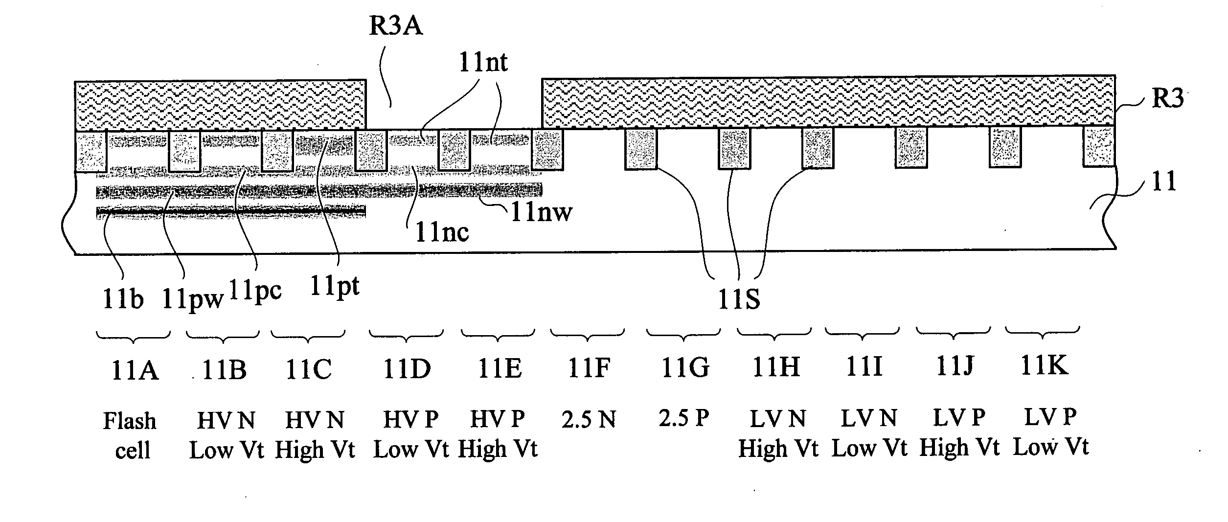
[0207] Referring to FIG. 15, the Semiconductor integrated circuit device 40 is a logic integrated circuit apparatus of 0.13 μm rule and including therein a flash memory device and includes device regions 41A-41K defined on a silicon substrate 41 of p-type or n-type by a device isolation insulation film 41S of STI structure, wherein a flash memory device is formed in the device region 41A, a high-voltage low-threshold n-channel MOS transistor is formed in the device region 41B, a high-voltage high-threshold n-channel MOS transistor is formed in the device region 41C, a high-voltage low-threshold p-channel MOS transistor is formed in the device region 41D, and a high-voltage high-threshold p-channel MOS transistor is formed in the device region 41E. These high voltage p-channel or n-channel MOS transistors constitute a control circuit controlli...

second embodiment

[0257] Next, the fabrication process of the semiconductor integrated circuit device according to a second embodiment of the present invention will be explained with reference to FIGS. 17A-17P, wherein those parts of drawings explained previously are designated by the same reference numerals and the description thereof will be omitted.

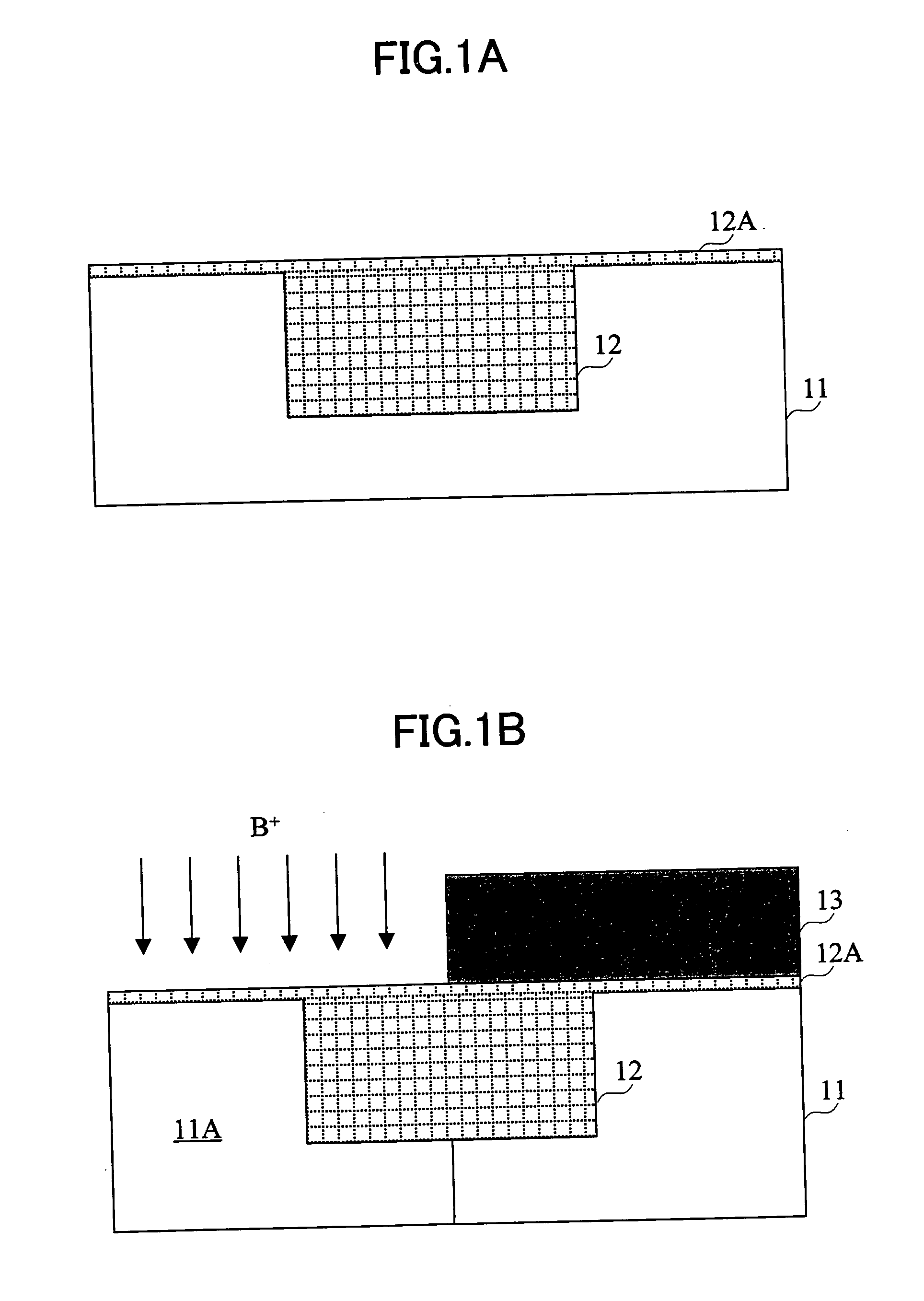
[0258] Referring to FIG. 17A, this process corresponds to the process of FIG. 16A before and there are formed device regions 41A-41K on the silicon substrate 41 so as to be defined by an STI device isolation insulation film 41S. Further, while not illustrated, the surface of the silicon substrate 41 is covered with a thermal oxide film of the thickness of 10 nm in the state of FIG. 17A.

[0259] Next, in step of FIG. 17B, a resist pattern R61 is formed on the structure of FIG. 17A so as to expose the device regions 41A-41C, and while using the resist pattern R61 as a mask, P+ is introduced to a depth 41b deeper than the bottom edge of the device isolatio...

third embodiment

[0280] Next, fabrication process of a semiconductor integrated circuit device according to a third embodiment of the present invention will be explained with reference to FIGS. 18A-18P, wherein those parts explained previously are designated by the same reference numerals and the description thereof will be omitted.

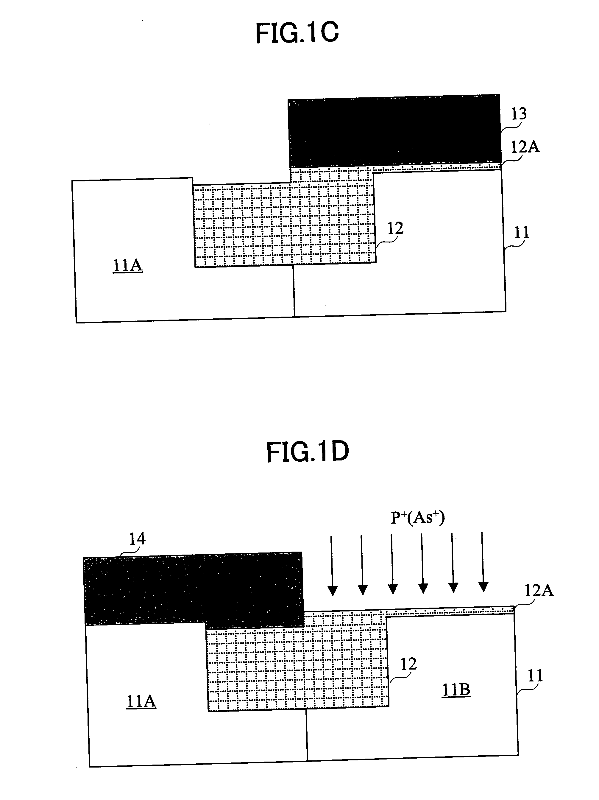
[0281] Referring to FIG. 18A, this process corresponding to the process of FIG. 16A or 17A noted before, and device regions 41A-41K are defined on a silicon substrate 41 by an STI device isolation insulation film 41S. Further, while not illustrated, the surface of the silicon substrate 41 is covered by a thermal oxide film of the thickness of 10 nm in the state of FIG. 18A.

[0282] Next, in the step of FIG. 18B, a resist pattern R81 exposing the device regions 41A-41C are formed on the structure of FIG. 18A, while using the resist pattern R81 as a mask, P+ is introduced to a depth 41b deeper than the lower edge of the device isolation insulation film 41S by an ion implant...


PUM


Abstract

An integrated circuit device comprises a memory cell well formed with a flash memory device, first and second well of opposite conductivity types for formation of high voltage transistors, and third and fourth wells of opposite conductivity types for low voltage transistors, wherein at least one of the fist and second wells and at least one of the third and fourth wells have an impurity distribution profile steeper than the memory cell well.

Description

CROSS-REFERENCE TO RELATED APPLICATIONS [0001] The present invention is a continuation application filed under 35 U.S.C.111(a) claiming benefit under 35 U.S.C.120 and 365(c) of PCT application JP2003 / 007373 filed on Jun. 10, 2003, the entire contents of each are incorporated herein as reference.BACKGROUND OF THE INVENTION [0002] The present invention generally relates to semiconductor devices and more particularly to a semiconductor integrated circuit device in which a nonvolatile memory device and a logic device are integrated and the fabrication process thereof. [0003] So-called hybrid semiconductor integrated circuit devices are the devices in which logic devices such as a CMOS device and non-volatile semiconductor memory devices such as a flash memory device are integrated on a common substrate. Such hybrid semiconductor integrated circuit devices constitute a product group called CPLD (complex programmable logic device) or FPGA (field programmable gate array), wherein these pro...

Claims


Application Information

Patent Timeline
Patent Type & Authority Applications(United States)
IPC IPC(8): H01L21/336H01L21/762H01L21/8238H01L21/8247H01L27/105H01L29/788
CPCH01L21/76237H01L21/823807H01L21/823878H01L27/11546H01L27/105H01L27/11526H01L21/823892H10B41/40H10B41/49
Inventor EMA, TAIJIKOJIMA, HIDEYUKIANEZAKI, TORU
Owner FUJITSU SEMICON LTD
Why Eureka
Try Eureka