Semiconductor device and manufacturing method thereof

a semiconductor and semiconductor technology, applied in the direction of semiconductor devices, electrical devices, transistors, etc., can solve the problems of large amount of oxygen, reduced heat and strength, and long oxidation time of about 15 hours, and achieves small device pitch, high reliability, and small chip size

Inactive Publication Date: 2006-02-23
FUJI ELECTRIC HLDG CO LTD
View PDF4 Cites 77 Cited by
  • Summary
  • Abstract
  • Description
  • Claims
  • Application Information

AI Technical Summary

Benefits of technology

[0023] In order to solve the above-described problems in the art, it is an object of the invention to provide a semiconductor device having high reliability, small device pitch and small chip size. Moreover, it is another object of the invention to provide a method of manufacturing a semiconductor device which is capable of forming...

Problems solved by technology

Such fixtures cause fatigue, contamination by foreign materials from a heater and strength reduction due to devitrification of the quartz fixtures.
Even with wet or pyrogenic oxidation, which is known to require a shorter oxidation time compared with that in dry oxidation though there is slight inferiority in quality of an obtained oxidized film, a long oxidation time of about 15 hours is still necessary.
Furthermore, in the above oxidation processing, a large amount of oxygen is introduced into a silicon wafer.
This introduces crystal defects such as oxygen deposits and oxidation induced stacking faults (OSF) and produces oxygen donors to thereby cause adverse effects such as characteristics deterioration and reliability degradation of a device.
It is known that a leakage current is increased in a p-n junction formed in a wafer with such crystal defects being introduced and a breakdown voltage and reliability are significantly degraded in an insulator film formed on the wafer by thermal oxidation.
Moreover, oxygen atoms taken in during diffusion processing become donors to cause an adverse effect of lowering a breakdown voltage.
This causes an adverse effect on reduction in device pitch and chip size.
This brings adverse effects such as an increase in lead time and the amount of maintenance.
The thick silicon oxide film causes adverse effects such as increase in cost, reduction in a rate of acceptab...

Method used


Image

  • Semiconductor device and manufacturing method thereof
  • Semiconductor device and manufacturing method thereof
  • Semiconductor device and manufacturing method thereof

Examples


embodiment 1

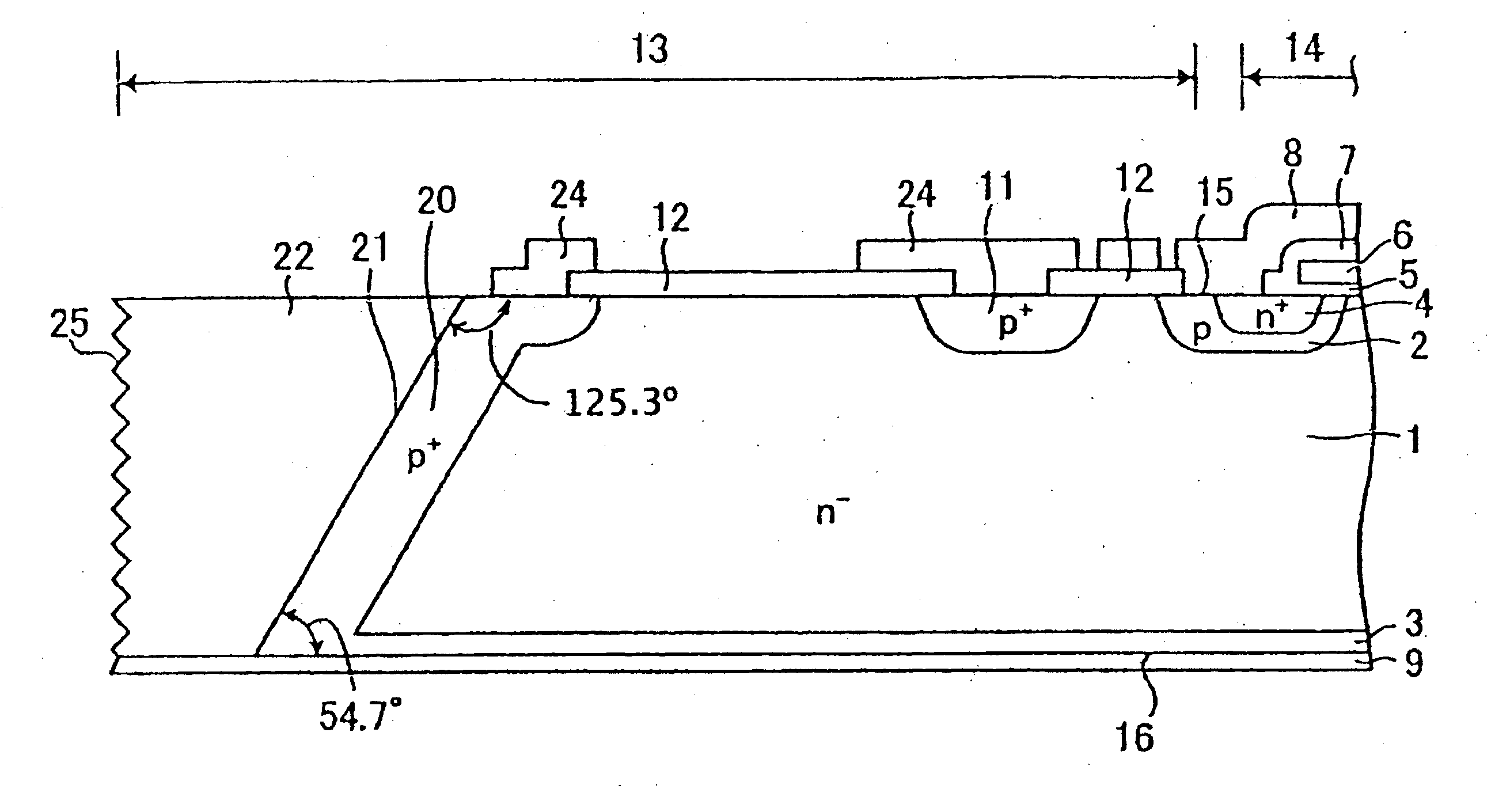
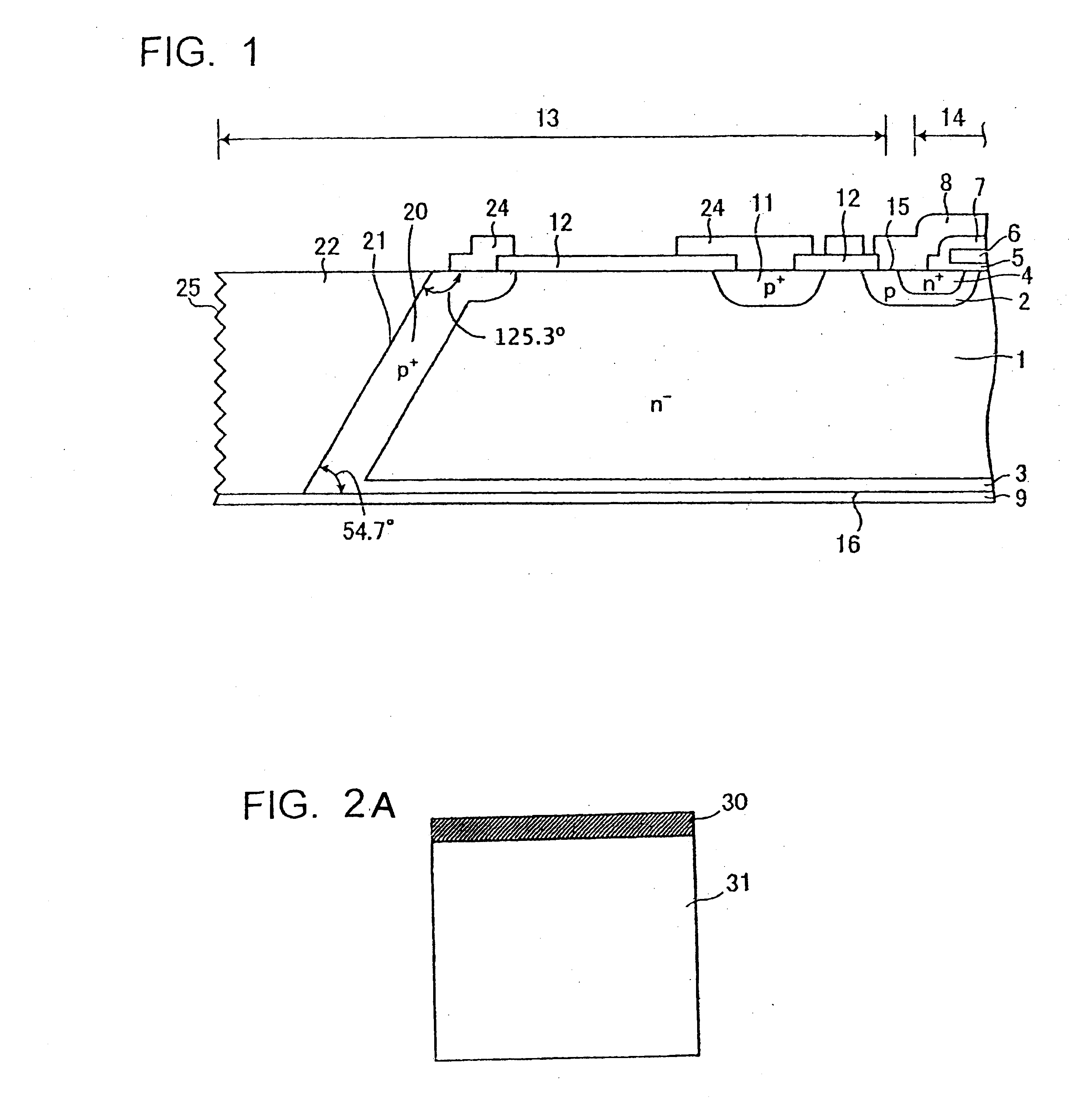
[0129]FIG. 1 is a cross sectional view showing an arrangement of a reverse-blocking IGBT according to embodiment 1 of the invention. As is shown in FIG. 1, on first principal surface 15 of n− silicon semiconductor substrate 1 with high resistivity, a plurality of p base regions 2 are selectively formed. On second principal surface 16 on a bottom surface side of the substrate, p+ collector layer 3 is formed. A region in between p base regions 2 and p+ collector layer 3 in the direction of the thickness of the substrate is originally n− single crystal silicon semiconductor substrate 1, which becomes an n base region. Although not particularly limited, the thickness of n− silicon semiconductor substrate 1, that is, the dimension from first principal surface 15 to second principal surface 16 is 200 μm, for example.

[0130] In active region 14 a part of which is shown by an arrow, n+ emitter region 4 is selectively formed in the surface layer in each p base region 2. On the outside of act...

embodiment 2

[0146]FIG. 3 is a cross sectional view showing an arrangement of a reverse-blocking IGBT according to embodiment 2 of the invention. As is shown in FIG. 3, the IGBT according to embodiment 2 has an arrangement in which, in the arrangement according to embodiment 1, filler region 22 between p+ isolation layer 20 and dicing face 25 is made to extend onto first principal surface 15 to cover voltage withstanding structure 13 and active region 14. The other arrangements are the same as those in embodiment 1. Therefore, as in embodiment 1, p+ isolation layer 20 can prevent a depletion layer, spreading around the p-n junction when the IGBT is reverse-biased, from expanding toward dicing face 25 and the damage region around it to allow the IGBT to obtain a sufficiently high reverse breakdown voltage. Elements similar to those in embodiment 1 are denoted with the same reference numerals and signs as those in embodiment 1, and explanations about these are omitted.

[0147] Next, a manufacturing...

embodiment 3

[0154]FIG. 10 is a plan view showing an arrangement of a thin semiconductor wafer in which a number of semiconductor chip forming areas of the semiconductor devices (here, reverse-blocking IGBTs) according to the invention are integrated. FIG. 11 is a cross sectional view showing an arrangement of a principal part of the semiconductor chip forming the area cut on line C-C in FIG. 10. FIG. 12 is an enlarged cross sectional view showing arrangements of the section D and the section E in FIG. 11. The thin semiconductor wafer is shown with the second principal surface of a thick semiconductor wafer, on the first principal surface of which a top surface structure is formed, being ground and with a bottom surface structure being formed on the ground second principal surface. No trench to be the scribing line and no isolation layer to be formed in the trench are therefore formed yet.

[0155] In IGBT chip forming area 135 on the side of first principal surface 131 of thin semiconductor wafer...


PUM


Abstract

A thin semiconductor wafer, on which a top surface structure and a bottom surface structure that form a semiconductor chip are formed, is affixed to a supporting substrate by a double-sided adhesive tape. Then, on the thin semiconductor wafer, a trench to become a scribing line is formed by wet anisotropic etching with a crystal face exposed so as to form a side wall of the trench. On the side wall of the trench with the crystal face thus exposed, an isolation layer for holding a reverse breakdown voltage is formed by ion implantation and low temperature annealing or laser annealing so as to be extended to the top surface side while being in contact with a p collector region as a bottom surface diffused layer. Then, laser dicing is carried out to neatly dice a collector electrode, formed on the p collector region, together with the p collector region, without presenting any excessive portions and any insufficient portions under the isolation layer. Thereafter, the double-sided adhesive tape is removed from the collector electrode to produce semiconductor chips. A highly reliable reverse-blocking semiconductor device can thus be formed at a low cost.

Description

CROSS REFERENCE TO RELATED APPLICATIONS [0001] This application claims priority from Japanese applications Serial Nos. JP PA 2004-240094, filed on Aug. 19, 2004, JP PA 2004-312590, filed on Oct. 27, 2004, and JP PA 2005-017486, filed on Jan. 25, 2005, the contents of all of which are incorporated herein by reference. BACKGROUND OF THE INVENTION [0002] A. Field of the Invention [0003] The present invention relates to a power semiconductor device used in a device such as a power conversion device and a manufacturing method thereof, and particularly to a process of forming an isolation layer in a bidirectional device or a reverse-blocking device having bidirectional voltage withstanding characteristics. [0004] B. Description of the Related Art [0005] In a semiconductor device of a reverse-blocking type, reverse-blocking capability equivalent to forward-blocking capability is required. In order to secure reverse-blocking capability, it is necessary to make a p-n junction holding a rever...

Claims


Application Information

Patent Timeline
IPC IPC(8): H01L29/80
CPCH01L21/6835H01L29/7393H01L29/045H01L29/0619H01L29/0646H01L29/0657H01L29/0661H01L29/0834H01L29/402H01L29/66333H01L29/7395H01L2221/68327H01L2221/68381H01L21/78H01L21/30608H01L29/0649H01L21/6836
Inventor SHIMOYAMA, KAZUOTAKEI, MANABUNAKAZAWA, HARUO
Owner FUJI ELECTRIC HLDG CO LTD
Why Eureka
Try Eureka