

Local ESD protection for low-capacitance applications
a low-capacitance, local technology, applied in the direction of diodes, semiconductor devices, electrical apparatus, etc., can solve the problems of thermal runaway in the device, ics may be severely damaged, onset of second breakdown, etc., to achieve robustness and easy manufacture
- Summary
- Abstract
- Description
- Claims
- Application Information
AI Technical Summary
Benefits of technology
Problems solved by technology
Method used
Image

Examples
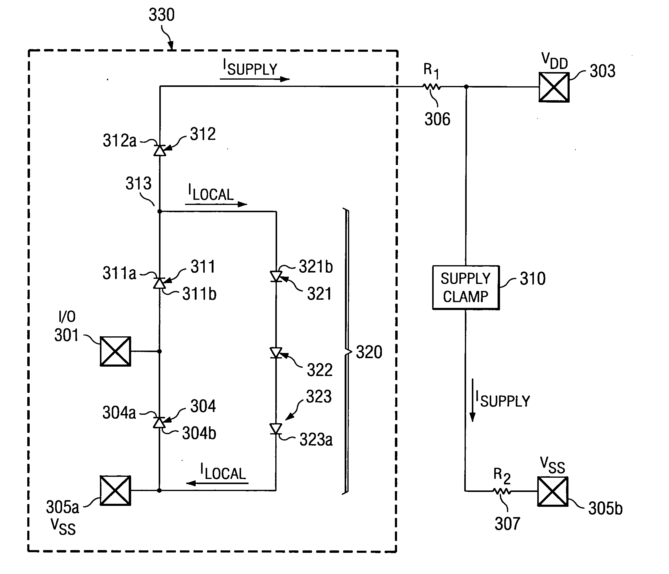
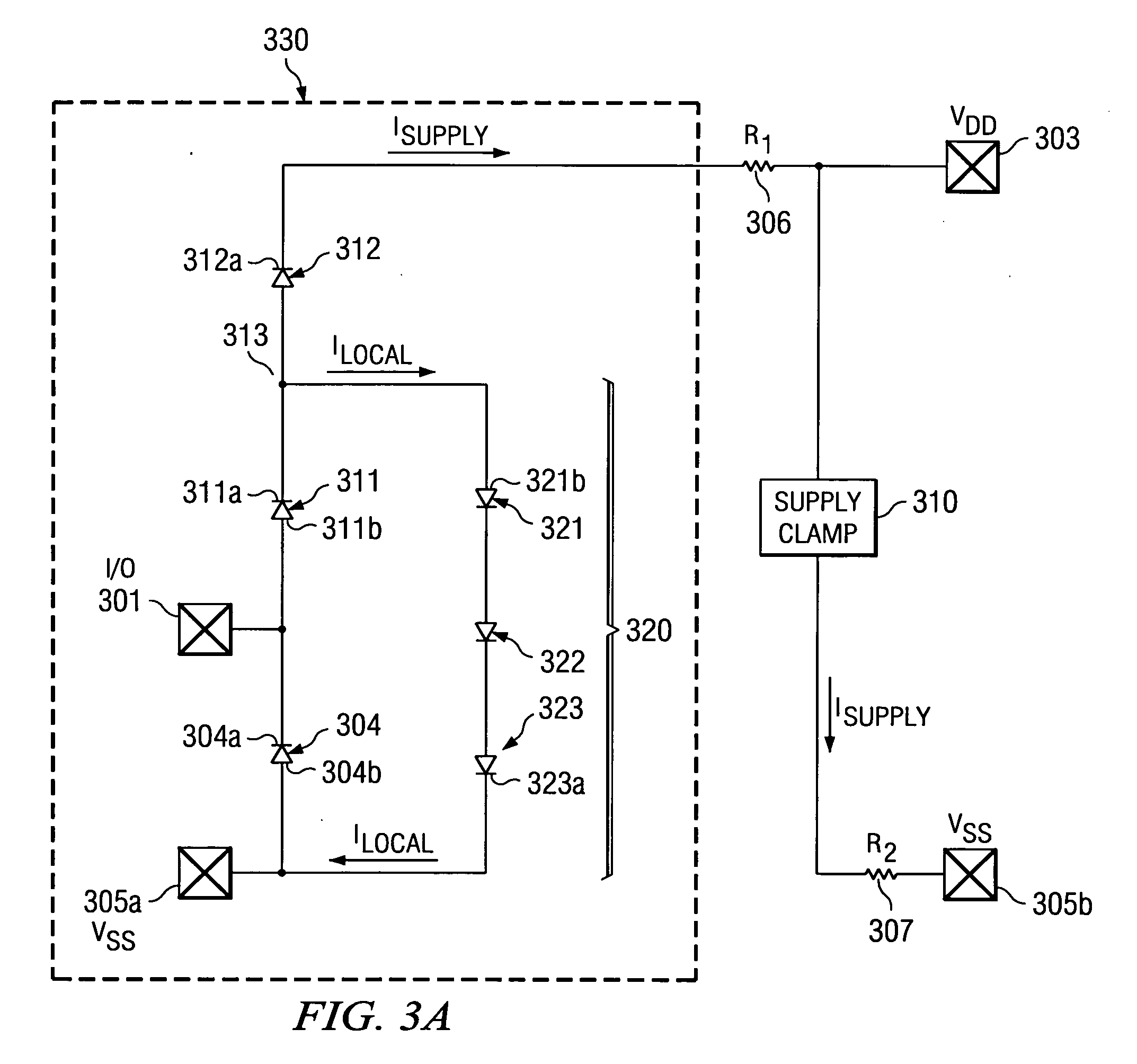
dashed outline 730
[0043] Dashed outline 730 in FIG. 7 marks schematically the components and functions, which can be geometrically accommodated in the area needed for I / O pad 701, creating the local ESD clamp.
[0044] Power pad 703 has a supply clamp 710 as ESD protection to ground (705b, Vss) through resistance 707 (second portion R2 of bus resistance). The local ESD clamp with transistor 720 does not rely on the supply clamp 710. As a matter of fact, approximately 70 to 85% of an ESD energy is discharged through the local clamp to ground, while only approximately 15 to 30% of the ESD energy is discharged through supply clamp 710 to ground. The effectiveness of the local clamp is thus independent of the bus resistance R=R1+R2.
[0045]FIG. 8 is a modified, and simplified, version of FIG. 7 in order to depict the formation and function of the silicon-controlled rectifier in more detail. The MOS transistor 820 is built in a substrate of first conductivity type. For many products, the first conductivity ty...
PUM
 Abstract
Description
Claims
Application Information