Micro fluid device and process for producing the same

Inactive Publication Date: 2006-05-04
KAWAMURA INST OF CHEM RES
View PDF6 Cites 30 Cited by
  • Summary
  • Abstract
  • Description
  • Claims
  • Application Information

AI Technical Summary

Benefits of technology

[0016] In the case of using a microfluidic device of the present invention as a microarray member for DNA analysis or immunodiagnosis and so forth, the fixed amount of probe can be made to be extremely large as compared with the prior art, thereby resulting in improved detection sensitivity, improved quantitativeness and faster analyses. In addition, since the porous resin layer having a three-dimensional mesh structure is formed as a spot inside the channel and a different probe can be fixed at each spot, multiple parameters can be analyzed with a single channel. Moreover, since the porous resin layer having a three-dimensional mesh structure is able to be formed only on the bottom surface of the channel, the surface of said porous resin layer can be optically observed throughout the channel, thereby enabling highly sensitive and highly quantitative measurements.
[0017] In the case of using a microfluidic device of the present invention as a reaction tank or reaction tube of a microreactor, since the fixed amounts of catalysts, enzymes and so forth can be increased, reaction speed and yield are improved. In addition, since the porous resin layer having a three-dimensional mesh structure can be formed at an arbitrary region inside the channel, and a different catalyst and so forth can be fixed at each region, multiple stages of reactions can be carried out with a single channel.
[0018] Since the use of a production process of the present invention eliminates the difficulty and restrictions of having to subsequently form a porous resin layer in a narrow channel, a microfluidic device having a porous resin layer having a three-dimensional mesh structure of uniform thickness on the surface of a channel can be easily produced without obstructing said channel on the inner surface of the minute channel of the microfluidic device. In addition, the thickness, pore shape and pore diameter of said porous resin layer can be easily adjusted to optimum values for the purpose of use. Moreover, a porous resin layer forming portion having a three-dimensional mesh structure of an arbitrary length, such as a spot-shaped porous resin layer portion, is easily provided in a portion of the channel in the direction of flow. In addition, there is no leakage of fluid inside the channel through a portion of the porous resin layer other than the porous resin layer on the bottom of the channel.
[0019] According to a production process of the present invention, since the pore diameter and thickness of a p

Problems solved by technology

In addition, since the fixation density of these inorganic materials is small in addition to the types of functional groups introduced onto the surface being limited, they still ended up being inadequate even if a porous body was employed.
Moreover, since silicon and metal are optically opaque, thereby preventing pigments and fluorescent pigments fixed to the inside of the porous body from being observed from the outside, they did not contribute to improvement of the sensitivity of light absorption or fluorescent detection.
Since these materials are optically opaque, there is a large amount of scattering of excitation light during fluorescence measurement, and since excitation light unable to be completely cut out with a filter ends up entering the receiving side, the baseline of measured fluorescent intensity becomes higher, thereby inviting a decrease in the S/N ratio and a decrease in reliability.
Moreover, sin

Method used


Image

  • Micro fluid device and process for producing the same
  • Micro fluid device and process for producing the same

Examples


example 1

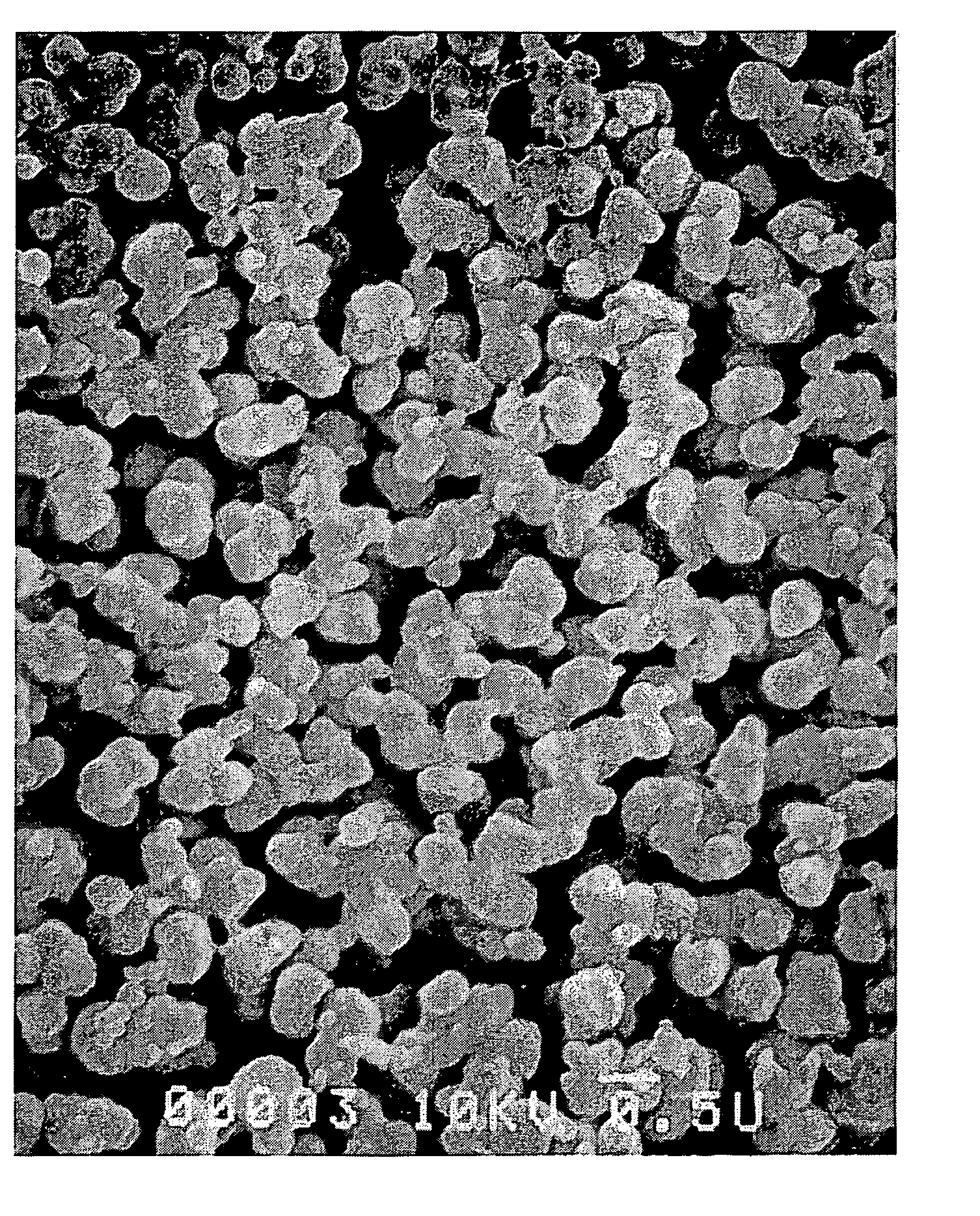
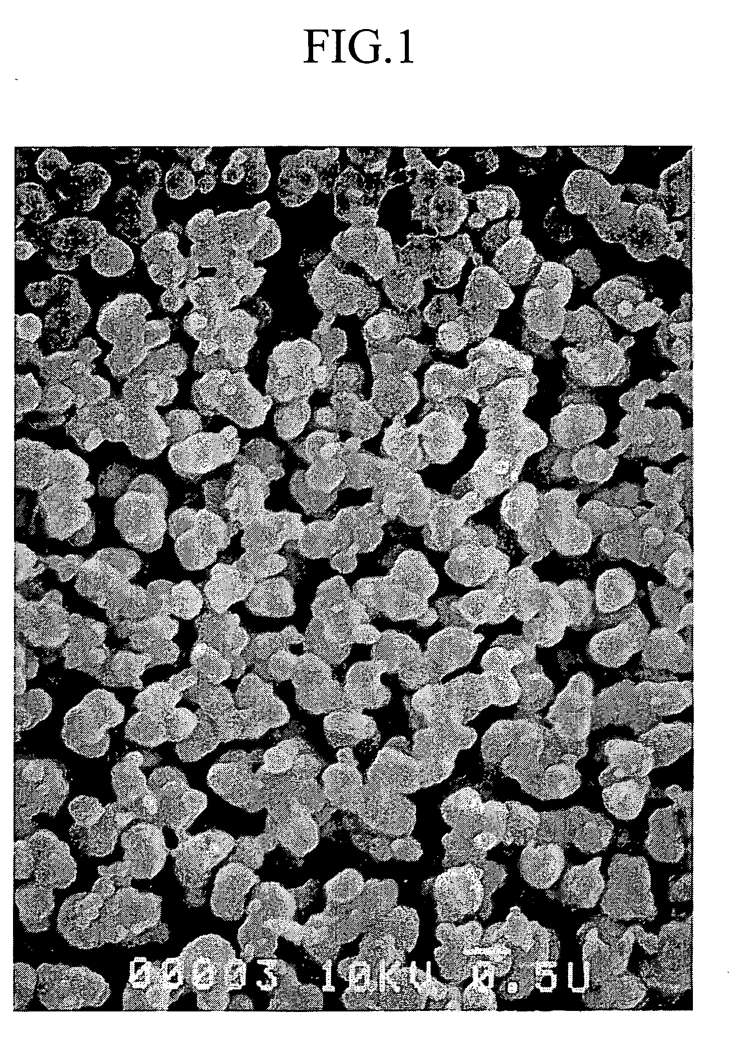
[0138] The present example 1 is an example of producing a porous resin layer having a three-dimensional mesh structure according to the “reaction induction-type phase separation method”.

[0139] [Preparation of Membrane Deposition Liquid (J)]

[0140] 72 parts of a trifunctional urethane acrylate oligomer (Unidic V-4263, Dainippon Ink and Chemicals) having an average molecular weight of 2000, 18 parts of dicyclopentanyl diacrylate (R-684, Nippon Kayaku), 10 parts of glycidyl methacrylate (Wako Pure Chemical Industries), 150 parts of methyl decanoate (Wako Pure Chemical Industries), 10 parts of a volatile good solvent in the form of acetone, and 3 parts of an ultraviolet polymerization initiator in the form of 1-hydroxycyclohexyl phenyl ketone (Irgacure 184, Ciba-Geigy) were uniformly mixed to prepare membrane deposition liquid (J1).

[0141] [Preparation of Composition (X)]

[0142] 50 parts of a trifunctional urethane acrylate oligomer (Unidic V-4263, Dainippon Ink and Chemicals) having an ...

example 2

[0162] The present Example 2 is an example of producing a porous resin layer having a three-dimensional mesh structure according to the “surface swelling method”.

[0163] [Preparation of Composition (X)]

[0164] A composition (X2) was prepared in the same manner as the preparation of composition (X1) in Example 1 with the exception of mixing 40 parts of 1,6-hexanediol ethoxylate diacrylate (Photomer 4361, Cognis Japan) instead of 40 parts of hexanediol diacrylate (New Frontier HDDA, Daiichi Pharmaceutical), and mixing 10 parts of nonylphenoxy polyethylene glycol (n=17) acrylate (N-177E, Daiichi Pharmaceutical) instead of 10 parts of glycidyl methacrylate (Wako Pure Chemical Industries). The viscosity of this composition was 220 mPa·s.

[0165] [Step 1: Formation of Porous Resin Layer Having a Three-Dimensional Mesh Structure]

[0166] (Formation of Three-Dimensional Mesh Structure)

[0167] After immersing a polystyrene sheet (Dainippon Ink and Chemicals) having a thickness of 150 μm used as ...

example 3

[0182] The present example 3 is an example of producing a porous resin layer having a three-dimensional mesh structure according to the “wet method”.

[0183] [Preparation of Membrane Deposition Liquid (K)]

[0184] 5 parts of a linear polymer in the form of an aromatic polyamide (Conex, Teijin), 90 parts of a solvent (U) in the form of N,N-dimethylacetoamide (Wako Pure Chemical Industries), and 5 parts of an additive in the form of ethylene glycol were uniformly mixed to obtain membrane deposition liquid (K).

[0185] [Preparation of Composition (X)]

[0186] 50 parts of tritetraethylene glycol bis-maleimide (Lumicure MIA200, Dainippon Ink and Chemicals), 40 parts of 1,6-hexanediol ethoxylate diacrylate (Photomer 4361, Cognis Japan), 10 parts of N,N-dimethylacrylamide (DMAA, Kohjin), and 0.5 parts of polymerization retardant in the form of 2,4-diphenyl-4-methyl-1-pentene (Kanto Chemical) were mixed to prepare composition (X3). The viscosity of said composition (X3) was 100 mPa·s.

[0187] [Ste...


PUM


Abstract

The object of the present invention is to provide a production process of a microfluidic device in which a porous resin layer, which is capable of optimally fixing a large amount of enzyme, antigen or other protein or catalyst on the inner surface of a minute channel of a microfluidic device without obstructing said channel, is formed at a uniform thickness on the surface of said channel. In the present invention, by preliminarily forming a porous resin layer having a large number of pores in its surface on a substrate, and forming an indentation having a porous resin layer on its bottom surface by using an activating energy beam-curable composition on said porous resin layer, followed by forming a channel by adhering a member serving as a cover to said indentation, a porous resin layer can easily be formed at a uniform thickness on the surface of said channel.

Description

TECHNICAL FIELD [0001] The present invention relates to a microfluidic device having a porous resin layer employing a three-dimensional mesh structure on the inner surface of a channel, and a production process thereof. BACKGROUND ART [0002] Attempts have begun in recent years to use microfluidic devices to analyze the components of fluids containing trace amounts of DNA, biological substances and so forth in various fields including medical diagnostics and biochemical testing. [0003] Microfluidic devices are also referred to as microfluid devices, microfabricated devices, lab-on-a-chip and micro total analytical systems (μ-TAS), and are capable of accelerating reactions and analyses, reducing the amounts of required reagents and reducing waste products by carrying out reactions and analyses in minute, capillary channels contained within the device. [0004] In the case of using such microfluidic devices to react with a sample in a fluid by fixing an enzyme, catalyst or functional gro...

Claims


Application Information

Patent Timeline
IPC IPC(8): B01D15/08B81C99/00G01N37/00G01N30/52G01N30/56G01N30/60G03F7/20
CPCG01N30/6052G01N30/6095G01N2030/525G01N2030/562Y10T137/2224
Inventor TAKADA, TETSUOANAZAWA, TAKANORIANAZAWA, ATSUSHI
Owner KAWAMURA INST OF CHEM RES
Why Eureka
Try Eureka