Charged particle beam apparatus and sample manufacturing method

Active Publication Date: 2006-05-11
HITACHI HIGH-TECH CORP
View PDF6 Cites 82 Cited by
  • Summary
  • Abstract
  • Description
  • Claims
  • Application Information

AI Technical Summary

Benefits of technology

[0014] In order to achieve the first object, it is necessary to arrange the ion beam irradiation system, the electron beam irradiation system, and the transmitting/scattered beam detection means in the vicinity of a sample so that the sample need not be moved for both of the FIB machining and the STEM observation. That is, the irradiation axis of the FIB irradiation system intersects the irradiation axis of the electron beam irradiation system for the STEM observation almost orthogonally and the sample is placed at the intersecting point so that the FIB cross section machining surface of the sample is defined by the thin film surface of the sample for the STEM observation. Moreover, the transmitted/scattered beam detection means is arranged backward of the sample viewed from the electron beam irradiation direction on the electron beam irradiation axis. By this arrangement, it is possible to realize the FIB machining and the STEM observation almost without moving the sample.
[0015] Next, explanation will be given on the means for achieving the aforementioned second object. From the first viewpoint for eliminating (or minimizing) the work such as a sample rotation work between the FIB machining stage and the STEM observation stage and simplifying the sample thickness optimization work using the STEM image monitor in the middle of the machining, the irradiation axis of the FIB irradiation system intersects the irradiation axis of the electron beam irradiation system for the STEM observation almost orthogonally. On the other hand, from the viewpoint for reducing the beam diameter in the FIB machining (high-speed machining and high machining position accuracy) and increasing the resolution of the STEM observation, the objective lenses of the electron beam irradiation system and the ion beam irradiation system should be arranged in the vicinity of the sample. However, because of the spatial size of the objective lenses o

Problems solved by technology

From the viewpoint of the STEM image observation, it is important to assure a sufficiently strong image signal and a high contrast but normally

Method used


Image

  • Charged particle beam apparatus and sample manufacturing method
  • Charged particle beam apparatus and sample manufacturing method
  • Charged particle beam apparatus and sample manufacturing method

Examples


first embodiment

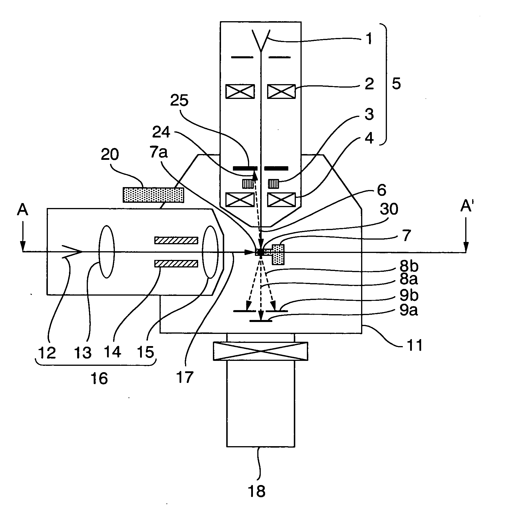
[0032]FIG. 1 shows a brief configuration of a charged particle beam apparatus according to the first embodiment of the present invention. FIG. 2 is a cross sectional view of FIG. 1 about A-A′.

[0033] The electron beam irradiation system 5 and the ion beam irradiation system 16 are mounted on a sample chamber case 11 so as to irradiate a sample 7. The electron beam irradiation system 5 includes a focusing lens 2 for focussing the electrons emitted from an electron gun 1, an electron beam deflector 3, and an objective lens 4 and has a function of irradiation of an electron beam 6 onto the sample 7 while reducing the beam diameter to a sufficiently small value and performing scan. On the other hand, the ion irradiation system 16 includes a focusing lens 13 for focusing ion emitted from the ion gun 12, an ion beam deflector 14, and an objective lens 15 and has a function of irradiation of a focused ion beam (FIB) onto the sample 7 while reducing the beam diameter to a sufficiently small...

second embodiment

[0046]FIG. 7 shows a brief configuration of the charted particle beam apparatus according to a second embodiment of the present invention. FIG. 8 explains an intersection angle between the electron beam irradiation axis and the ion beam irradiation axis. The charged particle beam apparatus according to the present embodiment is an example in which the intersection angle between the electron beam irradiation axis and the ion beam irradiation axis exceeds 90 degrees.

[0047] In this embodiment the intersection angle between the irradiation axes of the electron beam 6 and the ion beam 17 to the sample 7 is set to 110 degrees. Thus, as compared to the first embodiment in which the intersection angle is 90 degrees, the objective lens 15 of the ion irradiation system 16 can approach the sample by amount 3 mm and the FIB diameter can be reduced by about 15% when the machining beam performance has the same current calculation value. This is equivalent to that the FIB machining position accur...

third embodiment

[0049] When the objective lens of the electron beam irradiation system is a magnetic field type lens, the magnetic field is made to leak to the sample side so that the objective lens substantially approaches the sample, thereby increasing the STEM observation performance. The present embodiment is related to the leak magnetic field type objective lens, which will be detailed with reference to FIG. 9.

[0050] The objective lens 4 is a leak magnetic field type including a magnetic pole piece 4a and an excitation coil 4b. The magnetic field is made to leak to the sample side, i.e., the side of the intersection point 30 between the irradiation axis of the electron beam 6 and the irradiation axis of the ion beam 17 so as to form a magnetic flux density distribution 35 on the irradiation axis of the electron beam 6. The leaking magnetic field exists on the irradiation axis of the ion beam 17, too. FIG. 10 shows the magnetic flux distribution of the ion beam 17 on the irradiation axis. As t...


PUM


Abstract

It is possible to carry out a highly accurate thin film machining by irradiation of an ion beam to a sample and a high-resolution STEM observation of the sample by irradiating an electron beam with a high throughput almost without moving the sample. The FIB irradiation system has an irradiation axis almost orthogonally intersecting an irradiation axis of the STEM observation electron beam irradiation system. The sample is arranged at the intersection point of the irradiation axes. The FIB machining plane of the sample is extracted from the thin film plane of the STEM observation sample. The transmitting/scattered beam detector are arranged at backward of the sample on the electron beam irradiation axis viewed from the electron beam irradiation direction.

Description

BACKGROUND OF THE INVENTION [0001] 1. Field of the Invention [0002] The present invention relates to a charged particle beam apparatus enabling a user to observe the micro-sample extracted from, for example, a semiconductor device substrate while performing micro-machining and a sample fabrication method using the charged particle beam apparatus. [0003] 2. Description of the Related Art [0004] The technique of micro-machining using a focused ion beam (FIB) is disclosed, for example, in WO099 / 05506. By applying an FIB to a sample, it is possible to perform micro-machining using the sputtering phenomenon. Accordingly, it is possible to extract a micro-sample, for example, from a semiconductor device substrate. Moreover, by introducing a deposition gas into the vicinity of the FIB irradiation of the sample and performing the FIB irradiation in the gas atmosphere, a deposition film is formed by the ion beam assisted deposition phenomenon. This film formation can be used for a type of mi...

Claims


Application Information

Patent Timeline
IPC IPC(8): G21K7/00H01J37/08
CPCG01N1/32H01J37/26H01J37/28H01J2237/206H01J2237/2802H01J2237/30466H01J2237/3174H01J2237/31745H01J2237/31749
Inventor ISHITANI, TOHRUOHNISHI, TSUYOSHISATO, MITSUGUTAKEUCHI, KOICHIRO
Owner HITACHI HIGH-TECH CORP
Why Eureka
Try Eureka