Composite conductive film and semiconductor package using such film

a technology of composite conductive film and semiconductor package, which is applied in the direction of printed circuit manufacturing, printed circuit aspects, and nanoinformatics. it can solve the problems of unstable connection, disadvantage of two methods, and difficult filling of present underfill material into the spacing, so as to increase the strength of the 3d structure and high surface energy property

Inactive Publication Date: 2006-06-01
IND TECH RES INST
View PDF10 Cites 18 Cited by
  • Summary
  • Abstract
  • Description
  • Claims
  • Application Information

AI Technical Summary

Benefits of technology

[0012] According to the forgoing problems, a polymer conductive film and a semiconductor package using such film are provided in this specification. The polymer conductive film includes an anisotropic conductive film, having nanowires which are suitable for electrically connecting two chips that have little spacing there between. Among them, a high surface energy property of the nanowires is applied to reduce the required temperature and pressure, which will be in a metal diffusion bonding process. Also, a polymer material in the nanowire conductive film is applied for protecting said thin chip and for increasing the strength of the 3D structure. Besides, the conductive redistribution layer can be designed to solve the problem of the different input / output positions between stacked chips.

Problems solved by technology

However, a mismatch caused by the difference between the coefficient of thermal expansion (CTE) of the chip and that of the substrate makes the connection unstable.
Nevertheless, if spacing between the chip and the substrate is limited under 100 μm, the present underfill material will be hard to be filled into the spacing.
However, these two methods both have disadvantages.
Therefore it the stress can't be buffered.
About the second method, because a current conductive polymer still owns a resistivity ten times larger than metal, it is not suitable to be applied to an advanced and developed flip chip package which has tiny a space and a small electrode area.
Nevertheless, the thickness obtained by applying these two packaging techniques still is thicker in application.
However, the 3D stack package has the following problems: 1. lower stability, caused by the higher temperature and pressure used in a metal diffusion bonding process; 2. extra protection, required for preventing the thin chip from damage; 3. chips with different functions, having different input / output positions; 4. smaller spacing for input / output terminals, because the increased numbers of input / output terminals, when connecting multilayer chips; and 5. heat dissipation.
Nevertheless, rewiring the input / output to the edge of the bare chip may cause a decrease of the spacing for the input / output and decrease in the area for the input / output and therefore the difficulties of bonding process in chip stacking increase.
Therefore it hardly satisfies the high speed requirement of an advanced chip.

Method used


Image

  • Composite conductive film and semiconductor package using such film
  • Composite conductive film and semiconductor package using such film
  • Composite conductive film and semiconductor package using such film

Examples


first embodiment

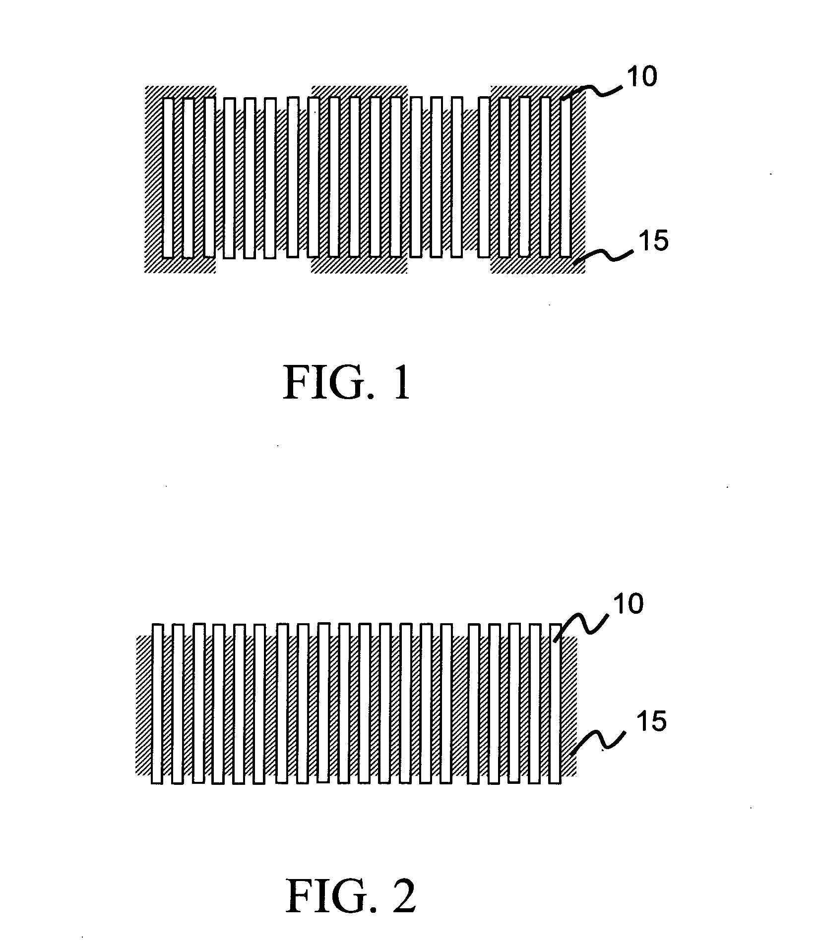
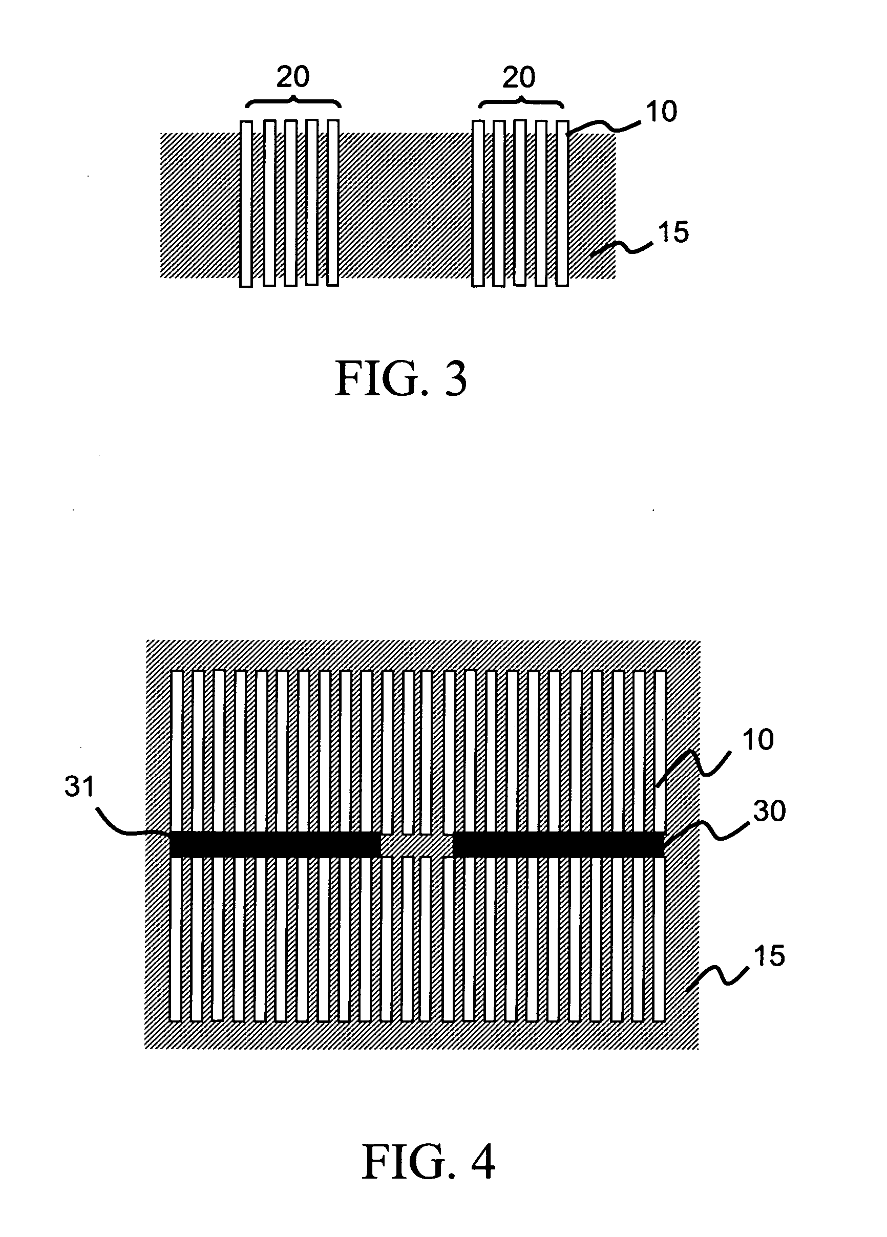
[0049]FIG. 1 is a cross section view of the polymer conductive film. The polymer conductive film has a plurality of wires 10 that are separated parallelly and have a Z direction conductivity and a spacing less than 200 nanometer, and a polymer material 15 filled between the wires 10 by a method such as a diffusion process. The wires 10 can include a high conductivity material such as gold, silver, cobalt or nickel. The polymer material 15 can include a thermoset polymer material, which has a small Young's modulus, for example, an epoxy or a polyimide.

[0050] Then, the polymer material 15 located on one side or both sides of the polymer conductive film has at least one opening, and one end or both ends of most wires 10 are exposed by the opening. The opening can be formed by a dry etching pattening process, such as plasma etching, to remove the polymer material 15 that is located at the predetermined bonding position between the polymer conductive film and the chip.

[0051] The polymer...

fourth embodiment

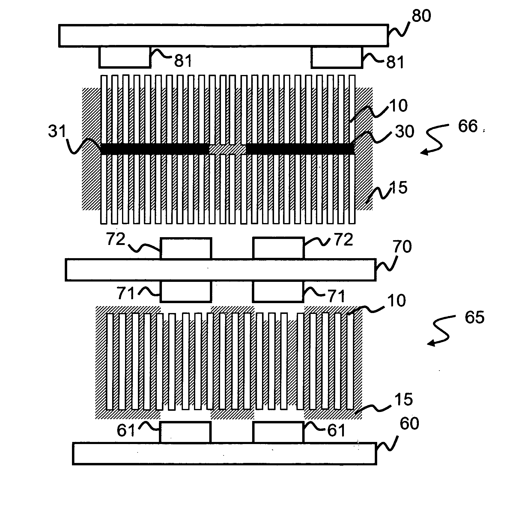
[0054]FIG. 4 is a cross section view of the polymer conductive film. The polymer conductive film is used as an electric connection between the chips. The chip to chip electric connection can be achieved by connecting the two chips respectively to at least one end of the wires 10 of the polymer conductive film. The polymer conductive film has a plurality of wires 10 that are separated parallelly and have a Z direction conductivity, a plurality of conductive redistribution layers 30, 31 and a polymer material 15 filled between the wires 10 by a method, such as a diffusion process. The conductive redistribution layers 30, 31 are formed on the conjunction surface between the wire layers 10 and can be spaced at equal or random intervals along the conductive direction. The wires 10 can include a high conductive material, such as gold, silver, cobalt or nickel. The polymer material 15 can include a thermoset polymer material 15, which has a small Young's modulus, such as an epoxy or a poly...

third embodiment

[0063] In FIG. 10, the polymer conductive film of the semiconductor package shown in FIG. 3 is used for being an electric connection between the substrate 40 and the chip 50, where the two ends of the wires 20 are exposed on the two sides of the third embodiment's polymer conductive film (please refer to FIG. 3) for being the electric connection between the substrate 40 and the chip 50. However, the parts outside the electrodes 41 of the substrate 40 and outside the electrodes 51 of the chip need an adhesive dispensing process to connect them to the polymer material 15 for increasing the strength of the package.

[0064] In FIG. 11, the polymer conductive film of the semiconductor package shown in FIG. 5 is used for being an electric connection between the substrate 40 and the chip 50. There are an electric pattern and electrodes 41 that have a plurality of input / output with larger spacing on the substrate 40, where the input / output electricity connects to the electric pattern. The ele...


PUM


Abstract

A composite conductive film and a semiconductor package using such film are provided. The composite conductive film is formed of a polymer-matrix and a plurality of nano-sized conductive lines is provided. The composite conductive film has low resistance, to connect between a fine-pitch chip and a chip in a low temperature and low pressure condition. The conductive lines are parally arranged and spaced apart from each other, to provide anisotropic conductivity. The present conductive film can be served as an electrical connection between a fine-pitch chip and a chip or a fine-pitch chip and a substrate.

Description

CROSS-REFERENCE TO RELATED APPLICATIONS [0001] This application is a continuation-in-part patent application of U.S. application Ser. No. 10 / 998,741 filed on Nov. 30, 2004, for “Structure of polymer-matrix conductive film and method for fabricating the same”. This application is also claims priority under 35 U.S.C. § 119(a) on Patent Application No(s). 094139773 filed in Taiwan, R.O.C. on Nov. 11, 2005. Each of theses application is incorporated herein by reference in its entirety.BACKGROUND [0002] 1. Field of Invention [0003] The invention relates to an anisotropic conductive film (ACF), especially to a composite conductive film that is made by polymers and nanowires. [0004] 2. Related Art [0005] In packaging techniques a variety of chip packages has been developed, such as a flip chip and a multi-chip module (MCM). Among them, the flip chip technology uses solder bumps to connect the input / output electrodes of the chip and the substrate. However, a mismatch caused by the differenc...

Claims


Application Information

Patent Timeline
Patent Type & Authority Applications(United States)
IPC IPC(8): H01L23/48
CPCB82Y10/00H01L23/49827H01L23/49866H01L23/49894H01L23/5384H01L25/0657H01L2224/16H01L2225/06513H01L2225/06517H01L2225/06572H01L2924/01079H01L2924/12044H01L2924/15174H05K3/323H05K2201/026H05K2201/10378Y10S977/762H01L24/29
Inventor UANG, ROUH HUEYCHEN, YU-CHIH
Owner IND TECH RES INST
Why Eureka
Try Eureka