Manufacturing method of insulating film and semiconductor device

a manufacturing method and technology of insulating film, applied in the direction of dielectric characteristics, instruments, optics, etc., can solve the problems of reduced adhesiveness between the top and bottom layers, mechanical strength of the interlayer insulating film, and difficulty in manufacturing semiconductor devices with high yield, so as to prevent damage, suppress parasitic capacitance between wires, and high yield

Inactive Publication Date: 2006-06-01
SEMICON ENERGY LAB CO LTD
View PDF20 Cites 81 Cited by
  • Summary
  • Abstract
  • Description
  • Claims
  • Application Information

AI Technical Summary

Benefits of technology

[0010] However, the CMP process is used in the Cu damascene method, and stress such as pressure from above and shear stress is thus applied to an interlayer insulating film. Accordingly, there are problems in that the mechanical strength of the interlayer insulating film, which can withstand the CMP process, and the adhesiveness with top and bottom layers are reduced.
[0011] In addition, the Cu damascene method has a polishing step, and thus variations in polishing easily occur in manufacturing steps of a semiconductor element over a large substrate such as a display device. This causes problems such as a short circuit between wires, and variations in the thickness of wires, leading to difficulty in manufacturing semiconductor devices with high yield.

Problems solved by technology

Accordingly, there are problems in that the mechanical strength of the interlayer insulating film, which can withstand the CMP process, and the adhesiveness with top and bottom layers are reduced.
This causes problems such as a short circuit between wires, and variations in the thickness of wires, leading to difficulty in manufacturing semiconductor devices with high yield.
On the other hand, an insulating film having a plurality of pores (porous insulating film) has a plurality of pores inside the film; therefore, there are problems in etching and an interface state with dissimilar materials.
Specifically, there is a possibility that an etching gas diffuses into an insulating film through pores and reacts in the insulating film when a contact hole is formed, leading to attachment of impurities and progress of etching in the insulating film.
As a result, it is difficult to manufacture semiconductor devices with high yield.
In addition, since the mechanical strength of a porous insulating film is extremely low, it is difficult to achieve both of low dielectric constant and mechanical strength capable of withstanding the CMP process, which results in reduced yield.

Method used


Image

  • Manufacturing method of insulating film and semiconductor device
  • Manufacturing method of insulating film and semiconductor device
  • Manufacturing method of insulating film and semiconductor device

Examples


embodiment mode 1

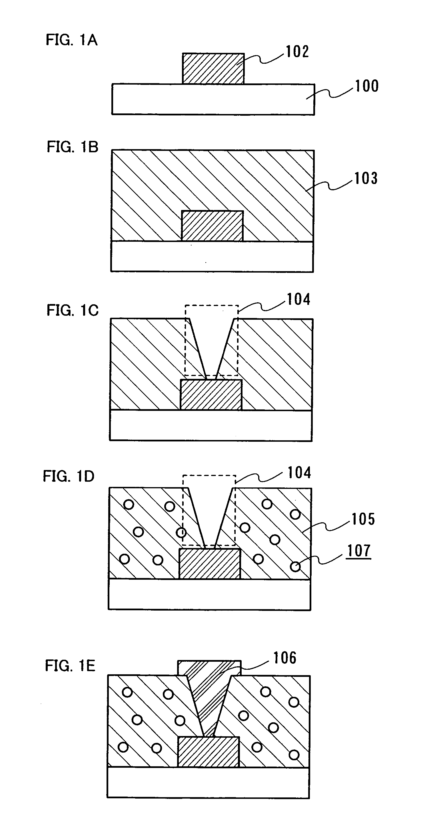
[0061] Described in this embodiment mode are a manufacturing method of an insulating film having pores (also called voids) and a forming method of a metal wire without using a CMP step. That is, description is made on a method where pores are formed using an fs laser after forming an insulating film. Description is also made on a method of forming a metal wire by discharging a composition containing a conductive material by a droplet discharge method.

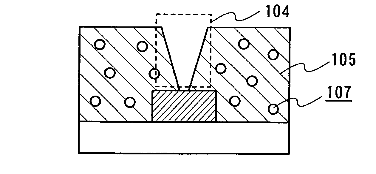
[0062] An embodiment mode of the invention is described with reference to FIG. 1A. This embodiment mode uses an insulating substrate 100 having elements such as transistors (not shown) formed by a common manufacturing process of a semiconductor device.

[0063] A metal wire 102 is formed over the insulating substrate 100. The metal wire 102 is obtained in the following manner. First, a metal film is formed by a known method such as printing, electroless deposition, electrolytic plating, PVD (Physical Vapor Deposition), CVD (Chemical Vapo...

embodiment mode 2

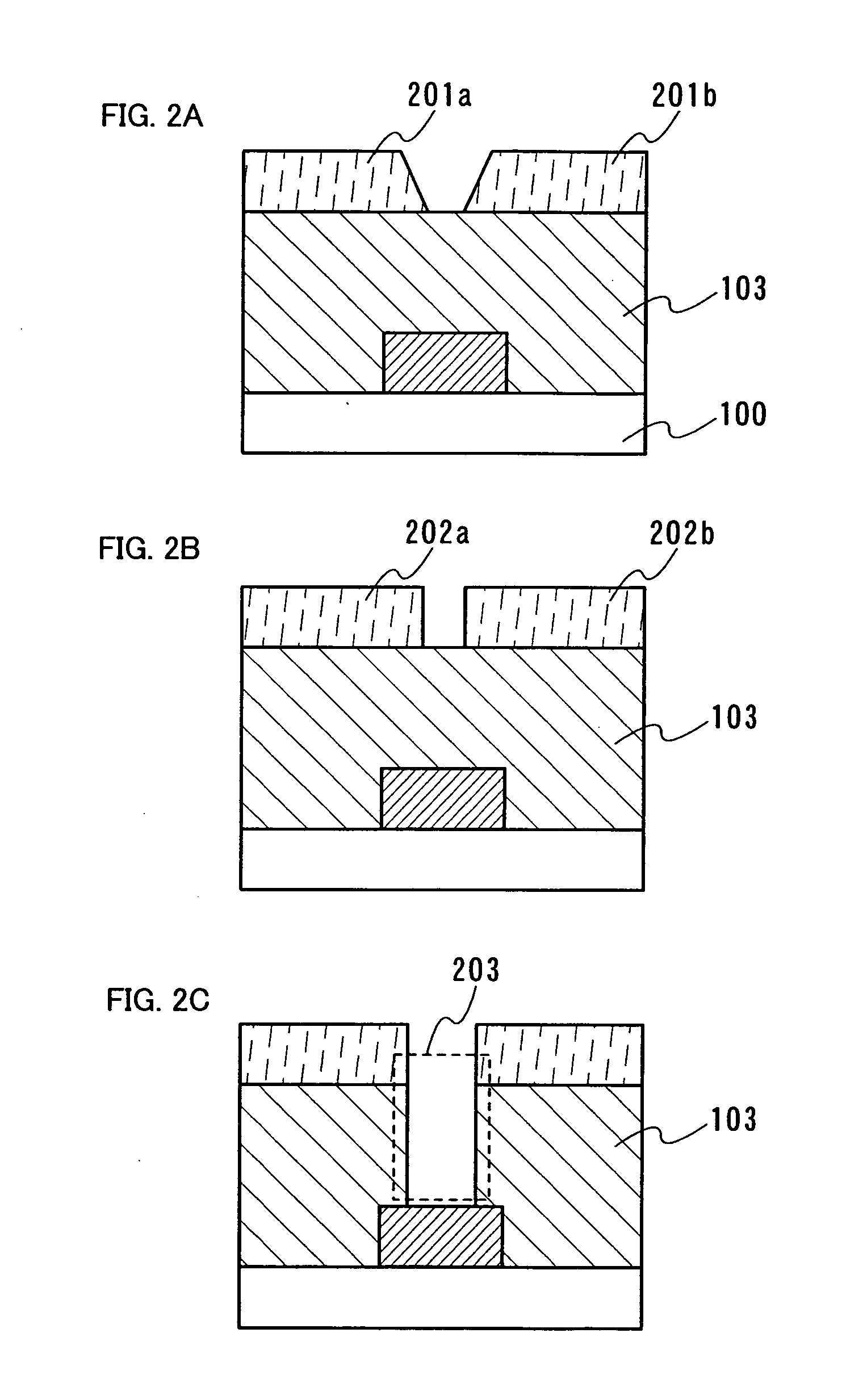
[0109] In this embodiment mode, forming steps of a porous insulating film and wires over a single crystalline semiconductor substrate are described with reference to FIGS. 10A to 10E.

[0110] As shown in FIG. 10A, element isolation regions 503 to 505 are formed over a substrate 500. The substrate 500 is a single crystalline semiconductor substrate or a compound semiconductor substrate, and typically, an N-type or P-type single crystalline silicon substrate, a GaAs substrate, an InP substrate, a GaN substrate, a SiC substrate, a sapphire substrate, a ZnSe substrate or the like. Instead, an SOI (Silicon On Insulator) substrate may be used. In this embodiment mode, a single crystalline silicon substrate is used as the substrate 500. The element isolation regions 503 to 505 may be formed by a known method such as a selective oxidation method (LOCOS: Local Oxidation of Silicon) and a trench isolation method. In this embodiment mode, silicon oxide films are formed as the element isolation ...

embodiment 1

[0119] Manufacturing steps of an active matrix substrate and a display panel having it are described with reference to FIGS. 1A to 11D, FIGS. 12A to 12C, and FIGS. 13 and 14. In this embodiment, a liquid crystal display panel is used as the display panel. FIG. 14 is a plan view of an active matrix substrate, and FIGS. 11A to 11D, FIGS. 12A to 12C and FIG. 13 are schematic views showing longitudinal cross sectional structures along a line A-B in a connecting terminal portion and lines C-D and E-F in a pixel portion of FIG. 14.

[0120] As shown in FIG. 11A, a first insulating film 801 with a thickness of 100 nm is formed on the surface of a substrate 800. In this embodiment, a silicon nitride film is formed by plasma CVD as the first insulating film 801. A first conductive film is formed over the first insulating film 801 and a mask is formed over the first conductive film. The first conductive film is etched using the mask to form a first conductive film 802a functioning as a gate wir...


PUM

PropertyMeasurementUnit
diameteraaaaaaaaaa
relative dielectric constantaaaaaaaaaa
porosityaaaaaaaaaa

Abstract

The invention provides a manufacturing method of an insulating film having a plurality of pores, as well as a manufacturing method of a highly integrated semiconductor device with high yield. According to the invention, a porous insulating film is formed by forming a plurality of pores in an interlayer insulating film using a laser beam, which results in lower dielectric constant of the interlayer insulating film. In addition, a composition containing conductive particles is discharged onto the porous insulating film by a droplet discharge method typified by an ink jet printing method, and then baked to form a wire. As the laser beam, an ultrashort pulse laser beam is preferably used.

Description

BACKGROUND OF THE INVENTION [0001] 1. Field of the Invention [0002] The present invention relates to a manufacturing method of a porous insulating film by use of a laser, and a manufacturing method of a semiconductor device having a wiring board and a semiconductor element by use of a droplet discharge method typified by an ink jet printing method. [0003] 2. Description of the Related Art [0004] In recent years, the thickness of a film constituting each part of a semiconductor element has been reduced for high integration of LSI (Large Scale Integrated circuit), and thus signal delay between multilayers has interfered with high speed operation. Since the signal delay depends on wire resistance and wire capacitance, a higher performance LSI requires a wiring material with a lower resistance and an interlayer insulating film material with a lower dielectric constant. [0005] In order to reduce the resistance of a wire, a copper (Cu) wire having a lower resistance has been properly stud...

Claims


Application Information

Patent Timeline
Patent Type & Authority Applications(United States)
IPC IPC(8): H01L21/31H01L21/324
CPCG02F1/136227H01L21/02126H01L2924/0002H01L21/02203H01L21/02362H01L21/288H01L21/31695H01L21/7682H01L21/76877H01L23/5329H01L27/12H01L27/3244H01L29/7833H01L2924/12044H05K3/0011H05K3/0035H05K2201/0116H05K2203/107H01L27/1248H01L27/1292H01L2924/00H01L2221/1047H10K59/12
Inventor YAMAMOTO, HIROKO
Owner SEMICON ENERGY LAB CO LTD
Why Eureka
Try Eureka