

Method of fabricating an epitaxially grown layer
a technology of epitaxial growth and layer, which is applied in the direction of crystal growth process, polycrystalline material growth, electrolytic capacitor, etc., can solve the problems of not being able to fabricate substrates from such ingots, not being able to obtain all materials, and existing methods not being suitable for fabricating gallium nitride (gan) ingots on an industrial scal
- Summary
- Abstract
- Description
- Claims
- Application Information
AI Technical Summary
Benefits of technology
Problems solved by technology
Method used
Image

Examples
example 1
Production of a Thick Epitaxially Grown Gallium Nitride Layer
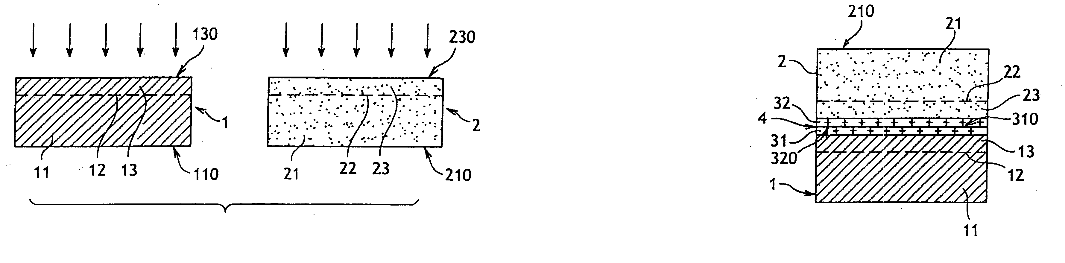
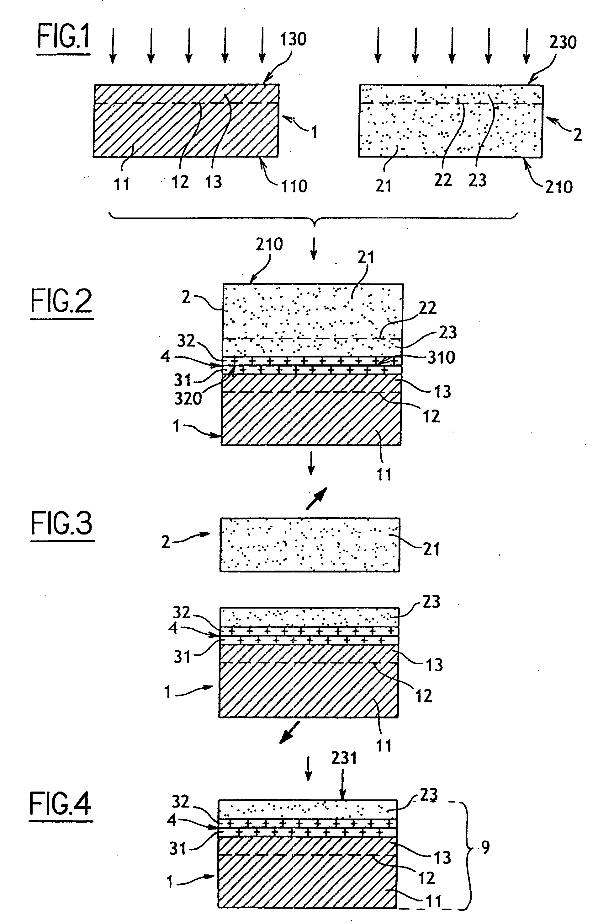
[0146] Hydrogen was implanted into a [111] silicon nucleation substrate 2 through a silicon oxide layer 32 obtained by thermal oxidation.
[0147] Hydrogen was also implanted onto a support substrate 1 formed from polycrystalline silicon carbide (SiC) through a layer of silicon oxide 31 obtained by deposition.
[0148] The implantation conditions for the silicon nucleation substrate 2 were an energy of 120 kilo electron-volts (keV) and a dose of 5×10¹⁶H+ / cm2, and for the SiC support substrate 1, the energy was 95 keV and the dose was in the range 1×10¹⁶H+ / cm2 to 4.5×10¹⁶H+ / cm2, preferably 3×10¹⁶H+ / cm2.
[0149] The silicon oxide layers 31 and 32 underwent chemico-mechanical polishing, CMP, to activate them and encourage their bonding by molecular bonding.
[0150] The remainder 21 of the [111] silicon layer was then detached by annealing at a temperature of 500° C. for two hours. It should be noted that the thermal budget applied...
example 2
Production of a Thick Epitaxially Grown Layer of Monocrystalline Cubic Silicon Carbide
[0156] Hydrogen was implanted into a monocrystalline [001] silicon nucleation substrate 2 through a silicon oxide layer 32 obtained by thermal oxidation.
[0157] Hydrogen was also implanted onto a support substrate 1 formed from polycrystalline silicon carbide (SiC) through a layer of silicon oxide 31 obtained by deposition.
[0158] The implantation conditions for the silicon nucleation substrate 2 were an energy of 120 keV and a dose of 5×10¹⁶H+ / cm2, and for the SiC support substrate 1, the energy was 95 keV and the dose was in the range 1×10¹⁶H+ / cm2 to 4.5×10¹⁶H+ / cm2, preferably 2×10¹⁶H+ / cm2.
[0159] The silicon oxide layers 31 and 32 underwent chemico-mechanical polishing (CMP) to activate them and to boost bonding by molecular bonding.
[0160] The remainder 21 from the [001] silicon layer was then detached by annealing at a temperature of 500° C. for two hours. It should be noted that the thermal ...
example 3
Production of a Thick Epitaxially Grown Gallium Nitride Layer
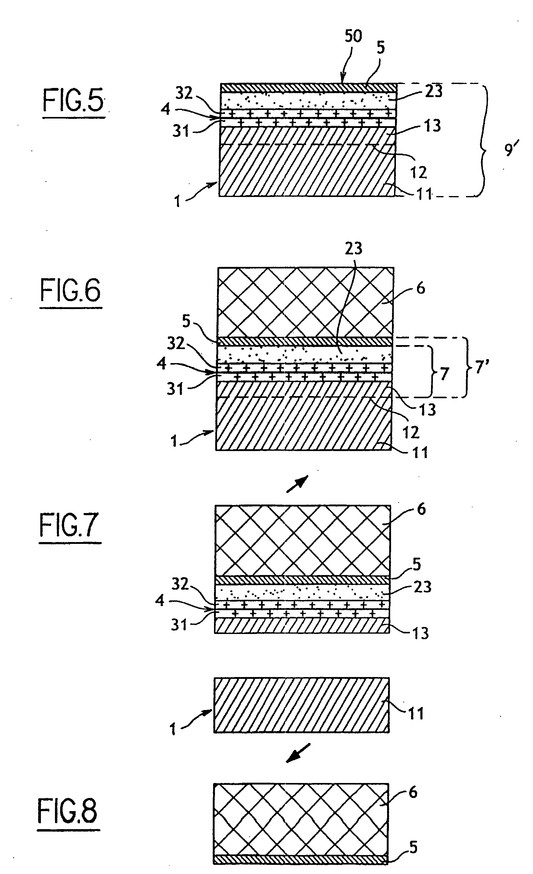
[0166] Hydrogen was implanted into a monocrystalline polytype 6H (hexagonal) silicon carbide support substrate 1′ through a sacrificial silicon oxide layer eliminated after implantation.
[0167] The implantation conditions were an energy in the range 50 to 200 keV, preferably 95 keV, and a dose in the range 1×10¹⁶H+ / cm2 to 4.5×10¹⁶H+ / cm2, preferably 3×10¹⁶H+ / cm2.
[0168] A thin layer 6′ of GaN was then grown epitaxially by MOCVD, said layer comprising an active zone for a light-emitting diode (LED). It should be noted that the thermal budget for said epitaxial growth (several hours of annealing between 700° C. and 1100° C.) was less than the energy budget necessary for subsequent detachment along the zone of weakness 12′.
[0169] The metal bonding technique described above was then used to transfer said epitaxially grown layer to an acceptor substrate 8 which can be silicon or copper.
[0170] After the bonding step, additiona...
PUM
| Property | Measurement | Unit |
|---|---|---|
| Thickness | aaaaa | aaaaa |
| Dielectric polarization enthalpy | aaaaa | aaaaa |
| Energy | aaaaa | aaaaa |
Abstract
Description
Claims
Application Information