Insulating gate AlGaN/GaN HEMT

Inactive Publication Date: 2006-06-29
CREE INC
View PDF30 Cites 41 Cited by
  • Summary
  • Abstract
  • Description
  • Claims
  • Application Information

AI Technical Summary

Benefits of technology

[0015] The present invention seeks to provide an improved AlGaN/GaN HEMT that addresses the above problems by having a thin AlGaN layer to reduce trapping and also having

Problems solved by technology

One disadvantage of Si is that it has low electron mobility (approximately 1450 cm2/V-s), which produces a high source resistance.
This resistance seriously degrades the high performance gain otherwise possible from Si based HEMTs.
However, GaAs has a relatively small bandgap (1.42 eV at room temperature) and relatively small breakdown voltage, which prevents GaAs based HEMTs from providing high power at high frequencies.
Despite these advances, AlGaN/GaN based FETs and HEMTs have been unable to produce significant amounts of total microwave power with high efficiency and high gain.
They produce significant power gain with DC gate drives, bu

Method used


Image

  • Insulating gate AlGaN/GaN HEMT
  • Insulating gate AlGaN/GaN HEMT
  • Insulating gate AlGaN/GaN HEMT

Examples


Embodiment Construction

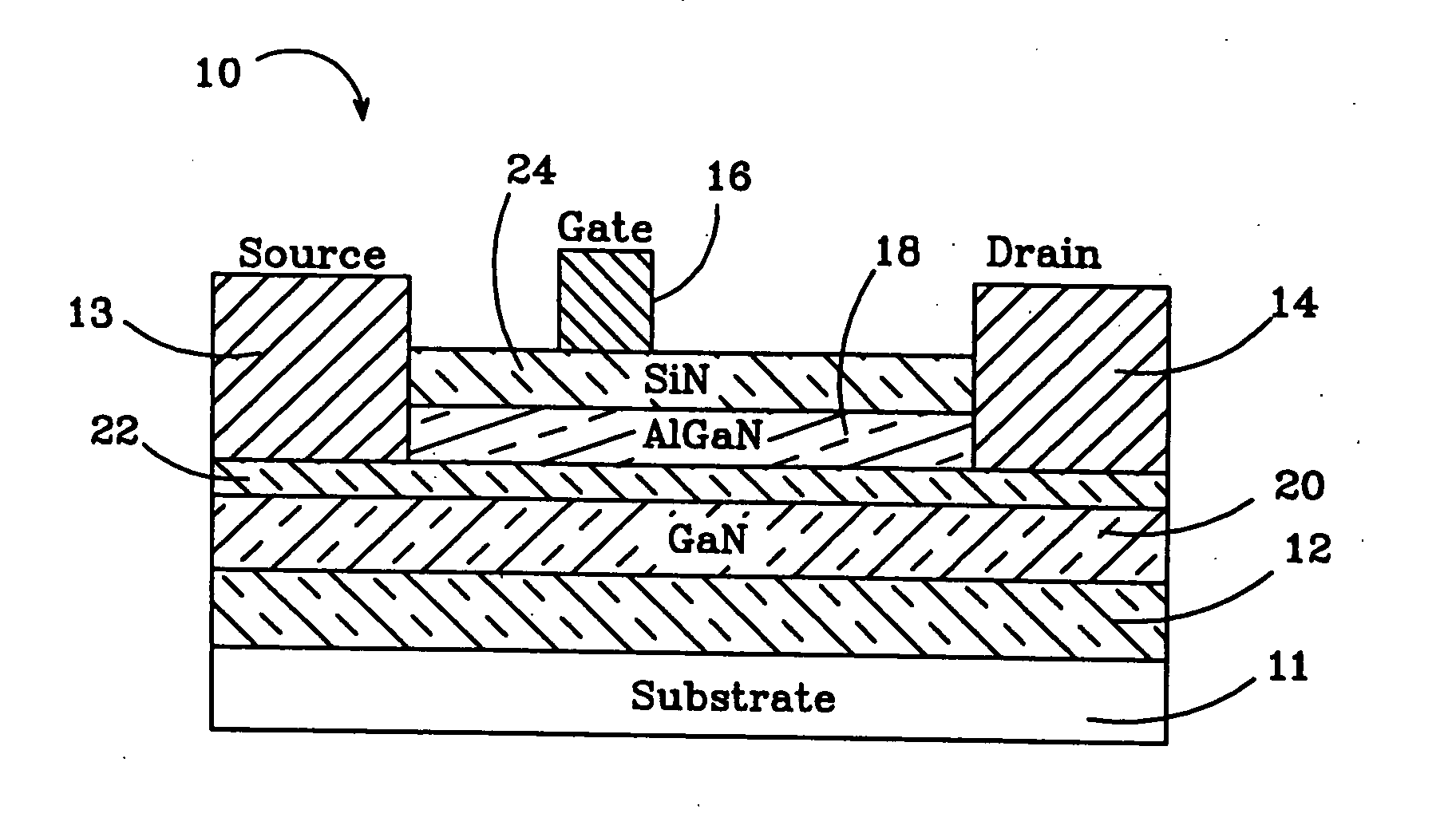
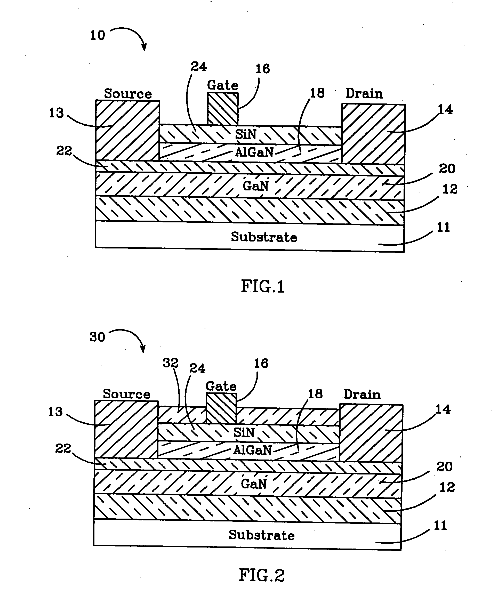
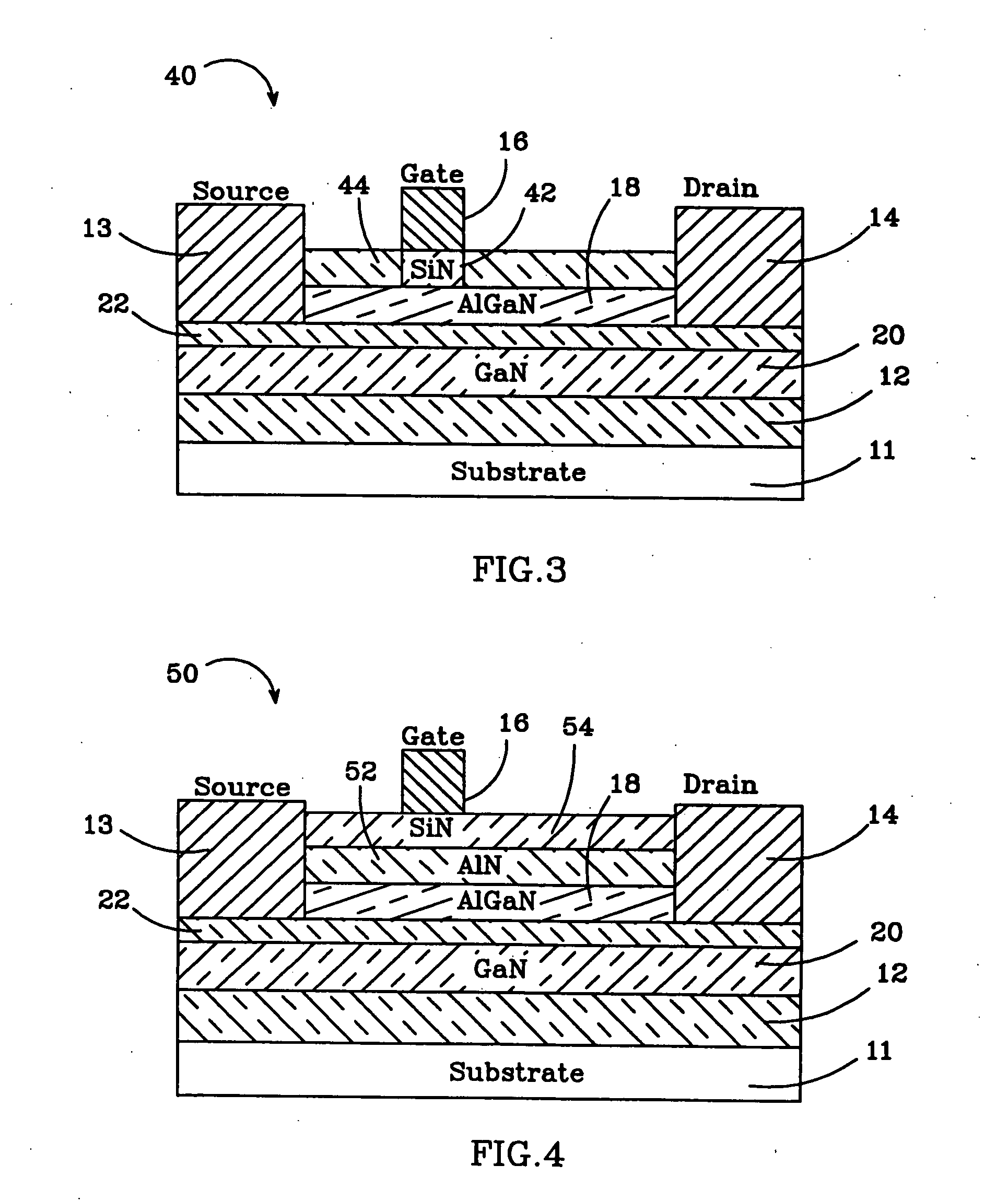
[0028]FIG. 1 shows an AlGaN / GaN based HEMT 10 constructed in accordance with this invention. It comprises a substrate 11 that can be either sapphire (Al2O3) or silicon carbide (SiC), with the preferred substrate being a 4H polytype of silicon carbide. Other silicon carbide polytypes can also be used including 3C, 6H and 15R polytypes. An AlxGa1-xN buffer layer 12 (where x in between 0 and 1) is included on the substrate 11 and provides an appropriate crystal structure transition between the silicon carbide substrate and the remainder of the HEMT 10. Many different materials can be used for the buffer layer 12 with a suitable material for a buffer layer on SiC being AlxGa1-xN, with x=1.

[0029] Silicon carbide has a much closer crystal lattice match to Group III nitrides than sapphire and results in Group III nitride films of higher quality. Silicon carbide also has a very high thermal conductivity so that the total output power of Group III nitride devices on silicon carbide is not l...


PUM


Abstract

AlGaN/GaN HEMTs are disclosed having a thin AlGaN layer to reduce trapping and also having additional layers to reduce gate leakage and increase the maximum drive current. One HEMT according to the present invention comprises a high resistivity semiconductor layer with a barrier semiconductor layer on it. The barrier layer has a wider bandgap than the high resistivity layer and a 2DEG forms between the layers. Source and drain contacts contact the barrier layer, with part of the surface of the barrier layer uncovered by the contacts. An insulating layer is included on the uncovered surface of the barrier layer and a gate contact is included on the insulating layer. The insulating layer forms a barrier to gate leakage current and also helps to increase the HEMT's maximum current drive. The invention also includes methods for fabricating HEMTs according to the present invention. In one method, the HEMT and its insulating layer are fabricated using metal-organic chemical vapor deposition (MOCVD). In another method the insulating layer is sputtered onto the top surface of the HEMT in a sputtering chamber.

Description

[0001] This application is a continuation of and claims the benefit of patent application Ser. No. 10 / 201,345, which claims the benefit of provisional application Ser. No. 60 / 307,546 filed on Jul. 24, 2001.BACKGROUND OF THE INVENTION [0002] 1. Field of the Invention [0003] This invention relates to aluminum gallium nitride and gallium nitride based high electron mobility transistors. [0004] 2. Description of the Related Art [0005] Microwave systems commonly use solid state transistors as amplifiers and oscillators which has resulted in significantly reduced system size and increased reliability. To accommodate the expanding number of microwave systems, there is an interest in increasing their operating frequency and power. Higher frequency signals can carry more information (bandwidth), allow for smaller antennas with very high gain, and provide radar with improved resolution. [0006] Field effect transistors (FETs) and high electron mobility transistors (HEMTs) are common types of s...

Claims


Application Information

Patent Timeline
IPC IPC(8): H01L29/739H01L21/335H01L29/812H01L21/338H01L29/20H01L29/778H01L29/78H01L31/0328
CPCH01L23/291H01L23/3171H01L29/2003H01L29/432H01L29/518H01L29/7787H01L2924/0002H01L2924/00H01L29/778H01L29/517H01L29/7786H01L29/7783
Inventor PARIKH, PRIMITMISHRA, UMESHWU, YIFENG
Owner CREE INC
Why Eureka
Try Eureka