

Display device and sputtering target for producing the same
a technology of sputtering target and display device, which is applied in the direction of discharge tube luminescnet screen, discharge tube details, instruments, etc., can solve the problems of increasing contact resistance, deteriorating the quality of displayed image, and reducing the electrical resistance of the display device, so as to achieve the effect of low electrical resistan
- Summary
- Abstract
- Description
- Claims
- Application Information
AI Technical Summary
Benefits of technology
Problems solved by technology
Method used
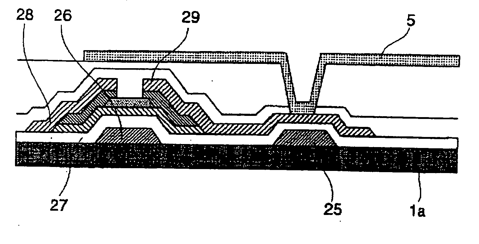
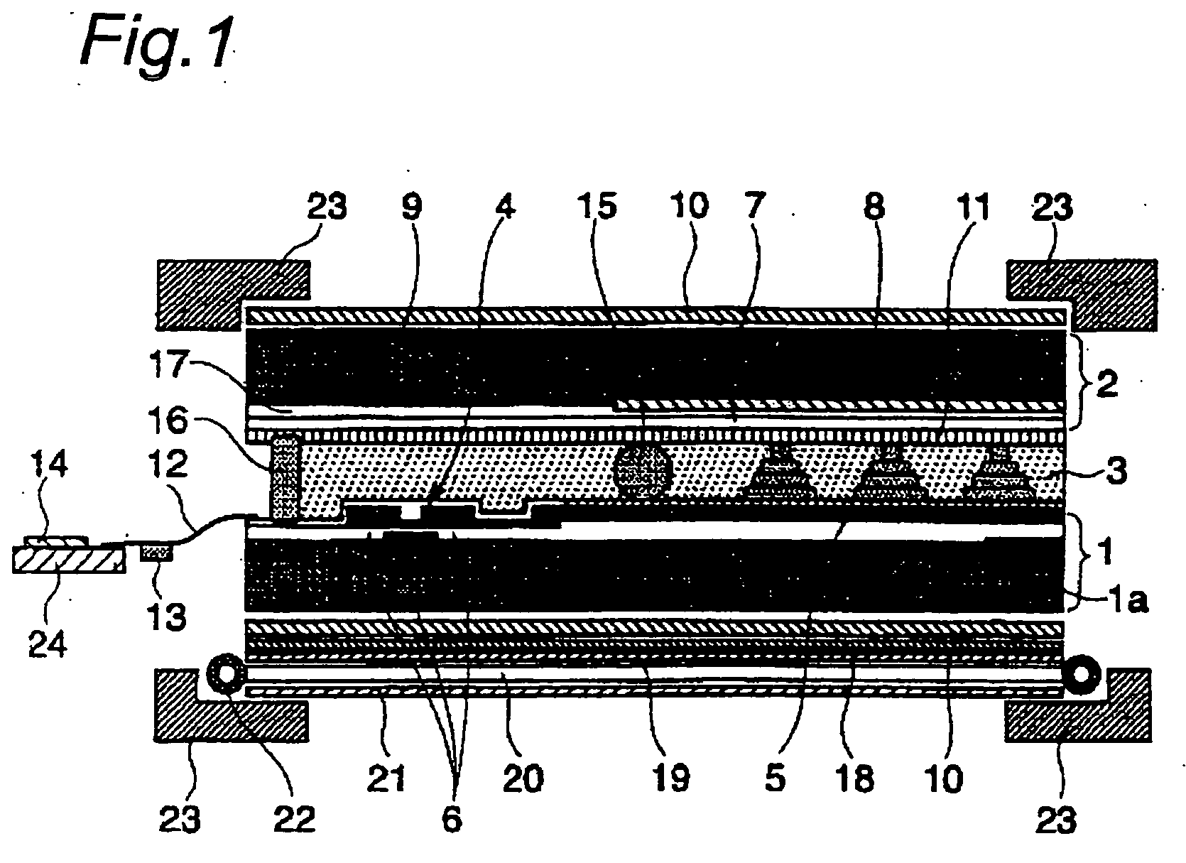
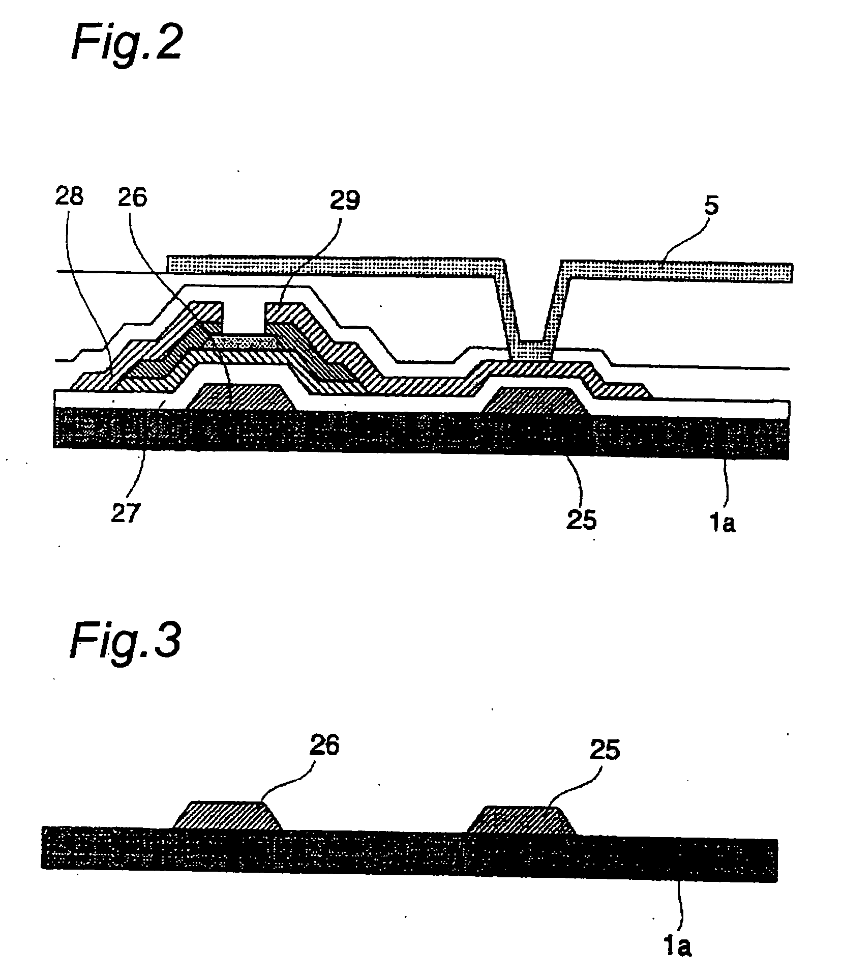
Image

Examples
example 1
[0116] With respect to the Al alloy films, which are shown in Tables 1, 3, 5, 7, 9 and 11, having various alloy compositions, the electrical resistances and the direct contact resistances with the Al alloy films brought in direct contact with pixel electrodes are measured and the heat resisting properties (hillock density) upon heating of the Al alloy films at 250 degrees Celsius for 30 minutes are investigated.
[0117] The experiment to obtain the measurements is as described below.
[0118] 1) Structure of the pixel electrodes: Indium tin oxide (ITO) obtained by adding 10 mass % tin oxide to indium oxide
[0119] 2) Thin film forming conditions: Gas atmosphere=Ar, Pressure=3 mTorr, Film thickness=200 nm
[0120] 3) Heating condition: 250 degrees Celsius×30 minutes
[0121] 4) Content of each element contained in Al alloy: Content of each element contained in Al alloys which are investigated in this Example was measured by using ICP (Inductive Coupled Plasma) emission spectrometry method.
[...
example 2
[0142] In this example, as described hereinafter, resistance against an alkaline solution using TMAH developing solution and presence or absence of a pitting corrosion were investigated about each sample of an Al alloy thin films having various alloy compositions listed in Tables 11 through 15.
[0143] In particular, Al alloy films were formed on glass substrates under the conditions described in 3) of above-described Example 1. Each of the Al alloy films obtained by the above step was directly immersed at 25 degrees Celsius in ordinary developing solutions (solutions containing 2.38 mass % TMAH), the time until the films got completely dissolved was measured, the etching rates per unit time (one minute) were calculated from thus measured time and the amounts of adhering films, and the resistance against an alkaline solution was evaluated in accordance with the following criteria. ∘: the etching rate slower than 40 nm / min, Δ: the etching rate of 40 nm / min or faster but slower than 70...
PUM
| Property | Measurement | Unit |
|---|---|---|
| electrical resistivity | aaaaa | aaaaa |
| temperature | aaaaa | aaaaa |
| electrical resistivity | aaaaa | aaaaa |
Abstract
Description
Claims
Application Information