[0009] The present invention may be better understood, and its numerous objects, features, and advantages made apparent to those skilled in the art by referencing the accompanying drawings.
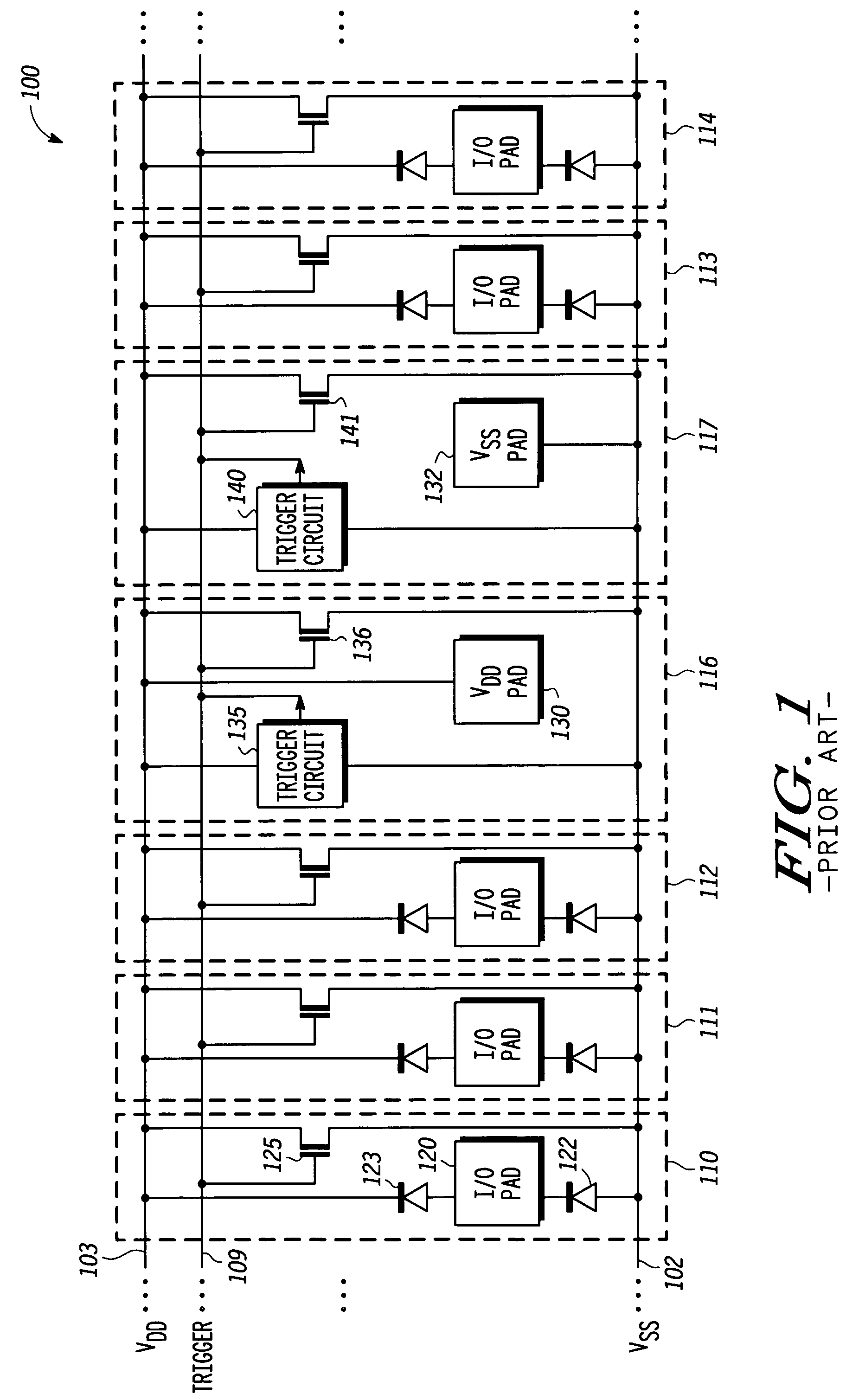
[0010]FIG. 1 is a circuit
schematic illustrating a prior art ESD protection network.
[0011]FIG. 2 is a circuit
schematic illustrating one embodiment of an ESD protection network according to the present invention.
[0012]FIG. 3 is a circuit
schematic illustrating another embodiment of an ESD protection network according to the present invention.
[0013]FIG. 4 is a schematic of one embodiment of an ESD trigger circuit according to the present invention.
[0014]FIG. 5 is a partial top view of one embodiment of active circuitry of an integrated circuit according to the present invention.
[0015]FIG. 6 is a circuit schematic illustrating another embodiment of an ESD protection network according to the present invention
[0016] The use of the same reference symbols in different drawings indicates identical items unless otherwise noted. The figures are not necessarily drawn to scale.
[0017] The following sets forth a detailed description of a mode for carrying out the invention. The description is intended to be illustrative of the invention and should not be taken to be limiting.
[0018] In one embodiment of the present invention, an ESD trigger circuit is located in every fourth or fifth I / O
cell of an I / O
cell bank while the remaining I / O cells of the bank include an ESD clamp NMOSFET (or another type of ESD clamp device), wherein the ESD trigger circuits drive the NMOSFETs in the neighboring I / O cells. With some embodiments, a trigger
bus is used to couple the output of the trigger circuit in a first type of I / O cells (i.e. those with trigger circuits) to the gates of the clamp NMOSFETs (or other type of ESD clamp devices) distributed in a second type of I / O cells (i.e. those with clamp NMOSFETs). In some embodiments, both types of I / O cells may be identical in all other respects. In some embodiments, an ESD trigger circuit in one I / O
cell of an I / O
cell bank may drive at least the two clamp NMOSFETs in adjacent I / O cells. At least some embodiments implement an ESD protection network such that a large bank of tightly abutted I / O cells may be protected without any intervening power or ground cells. Power and ground cells have been utilized for trigger cell placement in prior art ESD protection networks.
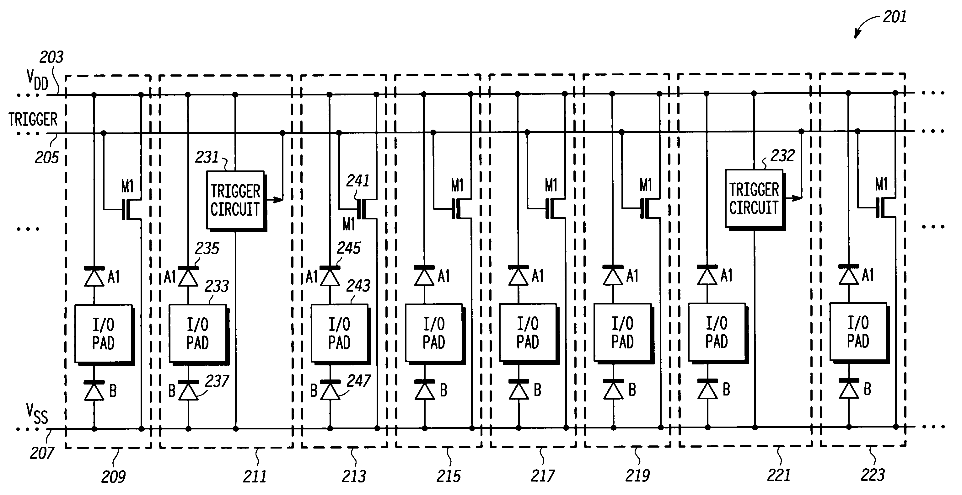
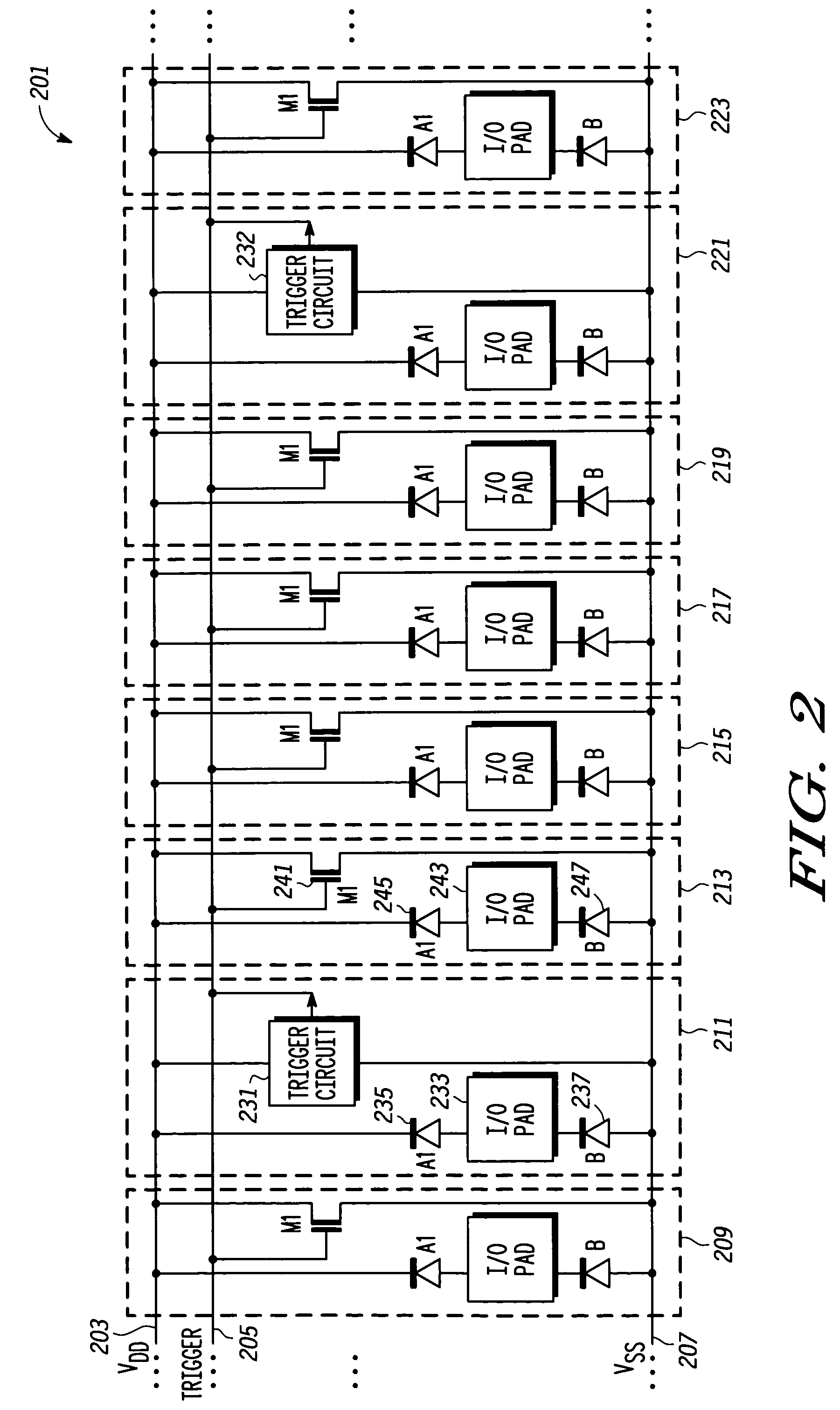
[0019]FIG. 2 illustrates an ESD protection network in a bank of I / O cells in an integrated circuit according to one embodiment of the present invention. Each I / O cell may be described in both a schematic sense, as shown in FIG. 2, and in a physical
layout sense (e.g. see FIG. 5), occupying a specific area in the IC periphery. As shown in the embodiment of FIG. 2, bank 201 includes I / O cells having an I / O pad and ESD elements. Not shown in the I / O cells of FIG. 2, but assumed present, is the I / O circuitry desired to be protected from ESD damage, such as for example P-channel MOSFET (PMOSFET) and N-channel MOSFET (NMOSFET) output drivers, input buffers, and other circuit components typically included for normal I / O operation. In one embodiment, bank 201 is part of a larger bank of I / O cells around the IC periphery region as indicated by the dots placed to the left and right of the elements shown in FIG. 2. The term “I / O cells” encompasses input-only cells, output-only cells, or input and output cells. The term “I / O pads” encompasses pads that convey only input signals, only output signals, or both input signals and output signals.
[0020] Each I / O pad (e.g. 243) is coupled to a VDD power supply
bus 203 via a
diode (e.g.
diode 245) designated as
diode A1 for each cell, and coupled to a VSS power supply
bus 207 via a diode designated as diode B (e.g. diode 247). In other embodiments, each I / O cell may include multiple pads such as two I / O pads or an I / O pad and a power pad (a
voltage or ground pad).
[0021]
Bank 201 includes two types of I / O cells. The first type of I / O cells (e.g. cells 211, 221), hereafter referred to as trigger I / O cells, include an ESD trigger circuit (e.g. 231, 232). The second type of I / O cells (e.g. cells 209, 213, 215, 217, 219, and 223), hereafter referred to as clamp I / O cells, include an ESD clamp device (designated as M1), which in the embodiment shown is implemented as an NMOSFET (e.g. NMOSFET 241). Other embodiments may include other types of ESD clamp devices e.g. a PMOSFET, a bipolar
transistor, or a
semiconductor controlled
rectifier (SCR).
[0022] Each ESD trigger circuit (231 and 232) in the trigger I / O cells (211 and 221) includes circuitry for detecting an ESD event. In one embodiment, an ESD event is defined as an event having a
rapid rise time characteristic of e.g. 100 picoseconds to 60 nanoseconds. However, an ESD event may be defined to have other rise times or by other characteristics in other embodiments. In response to detecting an ESD event, the trigger circuit drives the trigger bus 205 to approximately the
voltage level of VDD bus 203 to make conductive the M1 clamp devices of the clamp I / O cells (209, 213, 215, 217, 219, and 223) to
discharge the current of the ESD event from VDD bus 203 to VSS bus 207.
[0023] In one example showing the operation of the ESD protection network in bank 201, a positive ESD event is coupled to I / O pad 233 with respect to grounded VSS bus 207. This produces via forward biased A1 diode 235 a
voltage with a large
slew rate (dV / dt) on VDD bus 203. Trigger circuits 231 and 232 sense the rapid dV / dt on VDD bus 203, and in response drive trigger bus 205 to a voltage level approximately equal to the voltage level of the VDD bus 203, which makes conductive each of the M1 clamp NMOSFETs. In this manner the VDD bus 203 is discharged to ground via drain to source conduction of the multiple M1 clamp NMOSFETs which operate in parallel. The ESD network shown in FIG. 2 discharges other types of ESD events as well.
[0024] One
advantage of the embodiment shown in FIG. 2 is that all elements of the ESD network for protecting I / O
cell bank 201 reside within the I / O cells themselves. Note that no power or ground cells are needed for ESD protection in the embodiment of FIG. 2. This may be, in some embodiments, a significant improvement over prior art distributed rail clamp networks.
[0019]FIG. 2 illustrates an ESD protection network in a bank of I / O cells in an integrated circuit according to one embodiment of the present invention. Each I / O cell may be described in both a schematic sense, as shown in FIG. 2, and in a physical
layout sense (e.g. see FIG. 5), occupying a specific area in the IC periphery. As shown in the embodiment of FIG. 2, bank 201 includes I / O cells having an I / O pad and ESD elements. Not shown in the I / O cells of FIG. 2, but assumed present, is the I / O circuitry desired to be protected from ESD damage, such as for example P-channel MOSFET (PMOSFET) and N-channel MOSFET (NMOSFET) output drivers, input buffers, and other circuit components typically included for normal I / O operation. In one embodiment, bank 201 is part of a larger bank of I / O cells around the IC periphery region as indicated by the dots placed to the left and right of the elements shown in FIG. 2. The term “I / O cells” encompasses input-only cells, output-only cells, or input and output cells. The term “I / O pads” encompasses pads that convey only input signals, only output signals, or both input signals and output signals.
[0026]FIG. 3 illustrates another embodiment of a bank of I / O cells 301 of an integrated circuit according to the present invention. In the embodiment of FIG. 3, the ESD protection network includes an additional boost bus 302. In contrast to the network of FIG. 2, boost bus 302, rather than the VDD bus 303, powers the trigger circuits (e.g. trigger circuit 331 in I / O cell 315). Each I / O pad of bank 301 is coupled to boost bus 302 via an A2 diode (e.g. diode 329 in I / O cell 313).
[0027] A feature of this network is that the ESD trigger circuits are now coupled to any stressed I / O pad via boost bus 302 which is separate from the high ESD current VDD bus 303. During a positive ESD event applied, for example, to I / O pad 321 with respect to VSS bus 307 grounded, the primary (
high current) ESD path is through forward biased A1 diode 327 to the VDD bus, then through each of the M1 clamps to the VSS bus 307. Significant IR voltage drops occur along this path due to the high ESD current (e.g. 2-4 Amperes or greater), such that the M1 clamp NMOSFET drain to source voltage (Vds) is often one half or less of the voltage on the stressed I / O pad 321. A secondary (low current) ESD path is through forward biased A2 diode 329 to the boost bus 302, which powers the trigger circuits. The trigger circuits then detect a dV / dt transient on the boost bus 302 and drive the M1 clamp gates to approximately the boost
bus voltage via the trigger bus 305. Driving the M1 clamp gates requires very little current. Therefore, due to the very small ESD current routed along the boost and trigger buses, there is a
diode voltage drop (˜0.8V) due to the A2 diode, but very little IR
voltage drop between the stressed I / O pad 321 and the gates of the M1 clamps. Indeed the boost and trigger buses may be made quite narrow and resistive without imparting any significant IR drop during ESD events. Therefore, due to the fact that the trigger circuits are coupled to the stressed I / O pad via the low IR drop boost bus 302, rather than the high IR drop VDD bus 303, the gate to source voltage (Vgs) for the multiple M1 clamps is typically greater than the drain to source voltage (Vds). The on-resistance of a clamp NMOSFET is approximately inversely proportional to Vgs under these bias conditions. This helps to maximize the distributed rail clamp
network performance and minimize the
layout area required to implement robust ESD protection circuits of a given performance level. The “boosted” ESD network illustrated in FIG. 3 may provide enhanced ESD protection as compared to the non-boosted circuit shown in FIG. 2. A more detailed explanation and examples of boosted ESD protection networks may be found in U.S. Pat. No. 6,724,603.
[0028] As in the ESD network of FIG. 2, bank 301 comprises I / O cells of both types e.g. trigger I / O cells and clamp I / O cells. A single trigger I / O cell 315, with trigger circuit 331 is shown in FIG. 3. Also shown are multiple clamp I / O cells (e.g. 309, 311, 313, 317) with ESD clamp devices (implemented with NMOSFETs in the embodiment shown) designated M1 (e.g. 323). FIG. 3 shows five I / O cells in bank 301.
Bank 301 may contain additional I / O cells of both types as indicated by the three dots shown to the left of I / O cell 309 and to the right of I / O cell 317. In the ESD network of FIG. 3, every fourth or fifth I / O cell in the I / O bank contains a trigger circuit to drive the clamp NMOSFETs in the remaining nearby clamp I / O cells. However, in other embodiments the frequency of placement of trigger I / O cells among clamp I / O cells may vary.
Bank 301 may form a closed ring around the entire IC, or may form one of multiple I / O banks in the IC. Note that no power or ground cells are shown in FIG. 3. All elements of the ESD network for protecting the I / O
cell bank 301 reside within the I / O cells themselves.
[0029] In one embodiment, multiple ESD trigger circuits may operate in parallel to drive a single trigger bus (e.g. 305). In another embodiment, the trigger bus may be partitioned such that a single trigger circuit (e.g. 331) drives the trigger bus partition. In this embodiment, each ESD clamp device would be driven by a single trigger circuit. In other embodiments, a boost bus (e.g. 302) may be partitioned as well.
[0030] An
advantage of the ESD networks illustrated in FIGS. 2 and 3 is that they may enable robust ESD protection for IC designs without any ESD-specific rules for power or ground cell placement frequency within an I / O bank. This may greatly increase the design options and flexibility for the I /
O ring designer. In one embodiment, power or ground cells may be placed very infrequently in the I /
O ring (i.e. once for every 20 I / O cells or more). In another embodiment, the I /
O ring may not contain any power or ground cells, as may be the case for some integrated circuits bound for flip-
chip packages. With no requirements for ESD elements other than those found in the trigger and clamp I / O cells, the full active MOSFET rail clamp ESD protection circuitry for an I / O cell bank may be contained wholly within the physical extent of the I / O cells within the bank.
[0031]FIG. 4 is a
circuit diagram of one embodiment of ESD trigger circuit 331. Trigger circuit 331 includes an
RC circuit of capacitive element 405 and
resistive element 407 for detecting a dV / dt transient on the boost bus 302. If the voltage
rise time is sufficiently fast (e.g. 60 ns or less), transistor 409 is turned on long enough to pull node 410 down to the voltage of the VSS bus 307 (
logic level low).
Inverter 417 then outputs a voltage about equal to the boost bus 302 (logical level high) onto trigger bus 305 to turn on the M1 clamp devices (e.g. 323 in FIG. 3).
Current source 411 and capacitive element 415 act as a
delay-on circuit for holding the input of
inverter 417 low for a period of time appropriate to fully
discharge the ESD event (e.g. typically 300-600 ns for some embodiments).
[0032] In some embodiments, trigger circuit 331 may also include a VDD boost circuit (not shown in FIG. 4). A VDD boost circuit may be used to increase the boost
bus voltage to the voltage applied to the VDD bus during a positive ESD event applied directly to the VDD bus. The boost circuit may include a voltage
comparator circuit and if the voltage of the VDD bus exceeds the boost bus during an ESD event, the boost circuit pulls the boost bus up to the voltage of the VDD bus.
[0033]FIG. 4 shows one type of ESD trigger circuit that may be implemented in the ESD protection network of FIG. 3. This trigger circuit may be used for the non-boosted network of FIG. 2 by powering the trigger circuit with the VDD bus rather than the boost bus. Other embodiments may implement other types of ESD trigger circuits e.g. including other types of RC or transient
detector trigger circuits or voltage threshold
detector trigger circuits.
[0034]FIG. 5 is a partial top view of the physical layout of active circuitry (e.g. transistors, capacitors, resistors, diodes) of two I / O cells within an I / O cell bank (e.g. 301) of an integrated circuit 501. In one embodiment, the active circuitry includes devices having portions implemented in a
semiconductor material e.g. of the substrate as with bulk
semiconductor (e.g.
silicon, SiGe, GaAs) devices. In another embodiment, the
active devices may be implemented in
Silicon on Insulator (SOI) structures. FIG. 5 shows portions of the physical layout of the active area for two I / O cells: clamp I / O cell 313 and trigger I / O cell 315. It is assumed that other I / O cells (of both types) may be found to the right and left of the cells shown in FIG. 5. In one embodiment, I / O cells 313 and 315 are located in the periphery I / O ring of an IC.
[0035] As shown in FIG. 5, the active circuitry physical layouts for cells 313 and 315 are each laid out as per an active circuitry
floor plan, which is similar for both types of I / O cells. For example, the A1 diodes (327 and 337) of both cells are located in the same area of each floor plan. Also, the B diodes (e.g. 325 and 335), the A2 diodes (329 and 339), the NMOSFET buffers (buffer 507 of cell 313 and buffer 514 of cell 315) and PMOSFET buffers (buffer 505 of cell 313 and buffer 511 of cell 315) are located in the same areas of the floor plans. Also, cell 313 includes additional I / O circuitry 539 and cell 315 includes additional 110 circuitry 541, which are partially shown in FIG. 5, and are located in the same area of the floor plans.
[0036] In the embodiment shown, clamp I / O cell 313 includes M1 clamp device 323 located between NMOS output buffer 507 and PMOS output buffer 505. For other clamp I / O cells of bank 301 (e.g. cells 309, 311 and 317), the M1 clamp device is located in the same area of the floor plan as in cell 313.
[0037] In the embodiment shown, trigger circuit 331 of trigger I / O cell 315 is located in area 531 between NMOS output buffer 514 and PMOS output buffer 511. Area 531 resides in the same area of the active circuitry floor plan of trigger I / O cell 315 as M1 clamp device 323 resides within clamp I / O cell 313. Area 531 is shown in FIG. 5 including several
active devices (illustrated as rectangles) including, for example, capacitive element 405 and
resistive element 407. Device 545 is a PMOSFET
pull up transistor in
inverter 417. Other trigger I / O cells of bank 301, if present, also include an ESD trigger circuit located in the same area (e.g. 531) of the floor plan as in cell 315. Area 531 may include other devices in other embodiments.
[0038] In the embodiment of FIG. 5, M1 clamp device 323 in clamp I / O cell 313, and trigger circuit 331 in area 531 of trigger I / O cell 315, are of about the same physical size and occupy the same physical layout area of the floor plan of their respective I / O cells. For this reason, a design layout of a single base I / O cell floor plan may be created with nothing placed in this clamp / trigger circuit area. A clamp I / O cell or a trigger I / O cell can be designed from this base I / O cell floor plan by dropping in either an M1 clamp device (e.g. 323) or a trigger circuit (e.g. 331). A design for an I / O bank (e.g. I / O bank 301 in FIG. 3) may then be easily created by placing clamp I / O cells or trigger I / O cells as needed. This approach, utilizing a base I / O cell floor plan with interchangeable M1 clamp or trigger circuit provides a very efficient means of implementing the ESD network in a bank of I / O cells.
[0040] In some embodiments, trigger circuit 331 and M1 clamp device 323 occupy about the same layout area of the floor plans of the I / O cells. Otherwise, some area may be wasted in the I / O cell with the smaller of the two ESD elements, since the base I / O cell floor plan must accommodate the larger of the two ESD elements. Therefore, this equal area consideration may be a constraint when running ESD network circuit simulations in e.g. SPICE to determine the size of the M1 clamp devices, the size of the trigger circuit elements, and the optimum trigger circuit placement frequency (trigger I / O cell placement frequency) in a bank of I / O cells.
[0040] In some embodiments, trigger circuit 331 and M1 clamp device 323 occupy about the same layout area of the floor plans of the I / O cells. Otherwise, some area may be wasted in the I / O cell with the smaller of the two ESD elements, since the base I / O cell floor plan must accommodate the larger of the two ESD elements. Therefore, this equal area consideration may be a constraint when running ESD network circuit simulations in e.g. SPICE to determine the size of the M1 clamp devices, the size of the trigger circuit elements, and the optimum trigger circuit placement frequency (trigger I / O cell placement frequency) in a bank of I / O cells.
[0041] Referring again to FIG. 5, other I / O cells of other banks of an integrated circuit may have other physical layouts with different floor plans. For example, the layout of FIG. 5 shows the PMOSFET buffers (e.g. 505) and NMOSFET buffers (e.g. 507) intermixed with ESD circuitry (e.g. M1 clamp device, A1 diode, A2 diode, B diode, and trigger circuitry). However, in other embodiments, these areas may be separated from the ESD devices, or intermixed in other arrangements. Also in other embodiments, the ESD devices may be intermixed with other I / O circuitry (e.g. 539 and 541) of an I / O cell instead of being separate as shown in FIG. 5. Also in other embodiments, the floor plan of an I / O cell may have other forms than that shown in FIG. 5. For example, an I / O cell configured as input only need not include PMOSFET and NMOSFET output buffers. Other embodiments of I / O cells may include other circuitry.
[0042]FIG. 6 is a
circuit diagram of another embodiment of a bank of I / O cells 601 of an integrated circuit according to the present invention. The ESD protection network of FIG. 6 is similar to the ESD protection network of FIG. 3 except that the first type of I / O cells (e.g. 615) with ESD trigger circuits (e.g. 625) also includes a clamp device, designated as M2 clamp device (e.g. 621) and implemented with an NMOSFET. The second type of I / O cells (e.g. 613) are the same as before, with M1 clamp devices (e.g. 623). In one embodiment, the M2 clamp device occupies a smaller physical layout area of the I / O cell than that of the M1 clamp devices.
[0043] The embodiment of FIG. 6 is most efficient when the combined physical layout area of the trigger circuit 625 and M2 clamp device 621 is about equal to the physical layout area of the M1 clamp device (e.g. 623). Similar to the configuration described in reference to FIG. 5, a base I / O cell floor plan may be created which allows for interchangeable placement of either the combined trigger circuit and M2 clamp device (to make the first type of I / O cell) as e.g. in area 531 or the M1 clamp device (to make the second type of I / O cell).
[0044] For some IC applications, including an M2 clamp device and trigger circuit in the first type of I / O cell, and an M1 clamp device in the second type of I / O cell may advantageously provide for greater
discharge capability for the entire network while minimizing the physical layout area of the combined ESD elements.
