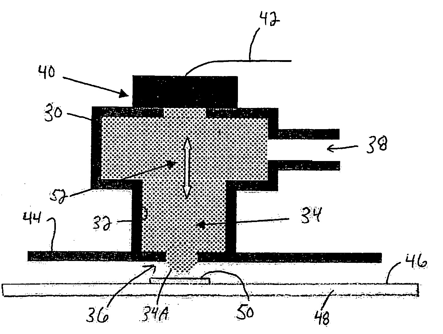
[0024] In certain preferred embodiments of the present invention, a method of making a microelectronic
assembly includes providing a microelectronic element having a front face and contact pads accessible at the front face, dispensing a mass of molten metal such as molten solder onto one of the contact pads of the microelectronic element, and applying ultrasonic energy or
waves to the mass of molten metal during the dispensing step for facilitating
wetting of the mass of molten metal with one of the contact pads of the microelectronic element.
[0031] Although not limited by any particular theory of operation, it is believed that the present invention provides an efficient and low cost method of making a microelectronic
assembly using a modified IBM C4NP tool set and using specially formulated
low melting point alloys. As is known to those skilled in the art, aluminum bond pads are not normally wettable by solder because of the presence of an
alumina film surface. The present invention seeks to solve this problem by using ultrasonic energy for breaking up the
oxide film by mechanical action, thereby facilitating direct
metallic bonding without using flux. Thus, the present invention equips a C4NP tool or a C4NP-like tool with an ultrasonic
transducer so that direct wetting of aluminum bond pads by a
low melting point alloy becomes possible. In certain preferred embodiments, the
low melting point alloy must be either fusible or rendered so through further alloying at the temperature at which the solder sphere is attached. As a result, the oxide
skin on the
fusible alloy can therefor be physically displaced. It has been determined that conventional fluxes will not work if the low
melting point alloy contains even ppm additions of aluminum. The low
melting point alloy should preferably contain a suitable mix of
major and minor elements to minimize the
solubility of aluminum and acts as a
diffusion barrier to intermixing of species in the solder with those on the
wafer and vice versa. Preferred low
melting point alloys include
tin,
zinc-based alloys,
indium,
bismuth and
cadmium based alloys.
[0032] In other preferred embodiments of the present invention, a method of making a microelectronic assembly includes providing a microelectronic element having a front face and contact pads accessible at the front face, providing a dispensing tool containing a molten metal such as molten solder and having a discharge port for dispensing the molten metal, and aligning the discharge port of the dispensing tool with one of the contact pads of the microelectronic element. The method preferably includes dispensing a mass of the molten metal through the discharge port and onto one of the contact pads of the microelectronic element, and applying ultrasonic
waves to the mass of molten metal during the dispensing step for facilitating wetting of the mass of molten metal with one of the contact pads of the microelectronic element.
[0035] In other preferred embodiments of the present invention, a C4NP tool or a tool similar to a C4NP tool may be used to disrupt, remove, dissolve or chemically reduce the aluminum oxide layer on an aluminum bond pad to facilitate wetting and bonding by a
solder alloy or molten metal. As described herein, in certain preferred embodiments, the
solder alloy wetted onto the bond pads is not a standard
solder alloy but contains other elements for modifying the reaction between a standard
tin-based solder and an aluminum bond pad. In one particular preferred embodiment, the thin film of solder applied to the bond pads may be a
zinc-based solder containing
nickel and
cobalt, to
restrict inter-
diffusion between the metals on the
wafer and those in the
flip chip solder spheres.
[0036] In certain preferred embodiments of the present invention, the aluminum bond pads on the
semiconductor wafer are manufactured to normal industrial standards, with the bond pads having smooth surfaces and being produced to high and consistent standards in terms of the metals and
process conditions used. As a result, the
alumina skin formed on the bond pads due to oxidation will generally be thin, probably less than 0.1 m thick and be of reproducible composition. Maintaining the consistency of the thickness and composition of the alumina skin will simplify the removal of the alumina skin and assist in ensuring consistent results.

