Method, system and apparatus for a time stamped visual motion sensor

a motion sensor and time stamp technology, applied in the field of visual motion detection, can solve the problems of small computational resource left for the computer, high computation load and data transfer load between the camera and the processor for large-scale 2-d arrays, etc., and achieve the effect of high resolution, high speed motion detection, and accuracy in velocity computation

Inactive Publication Date: 2006-09-07
BOARD OF RGT THE UNIV OF TEXAS SYST
View PDF4 Cites 97 Cited by
  • Summary
  • Abstract
  • Description
  • Claims
  • Application Information

AI Technical Summary

Benefits of technology

[0013] The present invention provides a method, system and apparatus for a time stamped visual motion sensor that provides a compact pixel size, higher speed motion detection and accuracy in velocity computation, high resolution, low power integration and reduces the data transfer and computation load of the following digital processor. More specifically, the present invention provides a new pixel structure based on a time stamped architecture for high-speed motion detection that solves many of the problems found in prior art devices. The relatively simple structure of the present invention, as compared to prior art structures, provides a compact pixel size results in a high resolution, low power integration. Moreover, the present invention does not use an in-pixel velocity calculation unit or an event-driven signaling circuit. Instead, the present invention uses an in-pixel time stamp component to record the motion transient time. Each pixel records the transient time of the motion edges asynchronously and then the information are read out frame by frame for post processing.
[0014] Measurement results show that the visual motion sensor using the time stamped architecture can detect motion information at 100 times higher time resolution than the frame rate. This enables much higher speed motion detection and greatly reduces the data transfer and computation load of the following digital processor. Moreover, the present invention can detect a wider range of motion speed by combining the timestamps in many consecutive frames together. As a result, the present invention can detect very fast and very slow movements (less than one pixel per sample period) at the same time without adjusting any device parameters or control signals. In addition, this structure is less sensitive to pixel mismatches and does not have the readout bottleneck problems found in FTI and event-driven signaling structures. As a result, the present invention provides higher accuracy in velocity computation with smaller pixel size and lower power consumption
[0015] More specifically, the present invention provides a visual motion sensor cell that includes a photosensor, an edge detector connected to the photosensor and a time stamp component connected to the edge detector. The edge detector receives inputs from the photosensor and generates a pulse when a moving edge is detected. The time stamp component tracks a time signal and samples a time voltage when the moving edge is detected. The sampled time voltage can be stored until it is read. In addition, the edge detector can be connected to one or more neighboring photosensors to optimize its sensitivity and robusticity.
[0016] The time stamp component may include a capacitor, a first, second, third and fourth switches, and a first and second D-flip-flop. The first switch is connected in series between a time input and the parallel connected capacitor. The second switch is connected in series between the parallel connected capacitor and the third switch. The third switch is controlled by a read signal and connected in series to a source follower, which is connected in series to an output node. The fourth switch is controlled by the read signal and connected in series between the output terminal of the second D-flip-flop and an odd frame signal node. The first D-flip-flop has a clear terminal that receives a reset signal, a clock terminal connected to the edge detector, a data terminal connected to a voltage source, a first output terminal that supplies a first output signal to control the first switch and a second output terminal that supplies an inverted first output signal to control the second switch. The second D-flip-flop has a clock terminal that receives the first control signal from the first D-flip-flop, a data terminal that receives an odd-even frame signal and an output terminal that supplies an inverted second output signal. Note that the second D-flip-flop can be replaced by storing the digital value onto with a transistor gate capacitor, which further reduces the layout area.

Problems solved by technology

However, both the motion computation load and the data transfer load between the camera and the processor for large scale 2-D arrays are very high.
This leads to a computational load as high as 4×10⁸×T, where T is the time required for comparing one pair of pixels.
Obviously, this is such a heavy load that there is very small computational resource left for the computer to perform other tasks required by the system application.
For more reliable results, an imaging processing algorithm such as block-matching may be used, which leads to even higher computational load.
As a result, the required computational resources may exceed the power of most computers.
Moreover, the power consumption associated with the load is often prohibitive, especially for battery powered portable devices.
However, there are still more issues to be resolved.
When the velocity is calculated based on RC constants of each pixel, the mismatch between the different pixels and the random noise make the calculated velocity inaccurate.
The second issue is the limited measurable speed range.
The third issue is in the readout of the motion information.
When sending out the speed vectors in each frame, the motion detectors can lose the information of the exact time point when the motion occurs within one frame.
This limits the performance of the motion sensor.
However, the additional processing circuits for pixel level motion computation normally result in large pixel size and high pixel power consumption, which largely limits the use of this kind of sensors.
Furthermore, the accuracy of measured motion velocity is also not good enough for some applications.
Although the FS architecture 200 can detect speed at each pixel, there are several major problems that prevent it to be used in real industrial or commercial products.
First, due to the serious mismatch and nonlinearity of the CMOS process, the detected speed is very inaccurate.
Second, the time constant of the charge or discharge process in each pixel is fixed during the testing, so the detectable dynamic range for the speed is very limited, i.e. it is not able to detect fast motion and slow motion at the same time.
This loss of information may be critical for some real time applications.
For a high integrated 2D array, it is not possible to measure the width of the pulse directly for each pixel.
Thus, the time resolution is still limited by the readout frame rate, as is the accuracy of speed measurement.
Although the pulse width for the detected Vr is accurate and much less dependent on the circuit mismatches, there are still some problems which limit the use of this kind of motion sensor.
That is, the accuracy of the speed measurement is still limited by the read out frame rate.
Secondly, since it is necessary to read out the sensor outputs at a very high frame rate to improve the accuracy of the speed measurement, it will occupy a big amount of time of the following computer or digital processor.
This also requires high bit rate data communication and high power consumption.
However, a major problem of this method is event confliction, which is serious when the array size is large.
In that case, a big amount of edges can occur within a very short period of time, which could exceed the maximum bandwidth of the output interface.
Even if the events are still been recorded after conflict-solving, the recorded event occurring time is not accurate because of the extra delay caused by the confliction.

Method used


Image

  • Method, system and apparatus for a time stamped visual motion sensor
  • Method, system and apparatus for a time stamped visual motion sensor
  • Method, system and apparatus for a time stamped visual motion sensor

Examples


Embodiment Construction

[0060] While the making and using of various embodiments of the present invention are discussed in detail below, it should be appreciated that the present invention provides many applicable inventive concepts that can be embodied in a wide variety of specific contexts. The specific embodiments discussed herein are merely illustrative of specific ways to make and use the invention and do not delimit the scope of the invention.

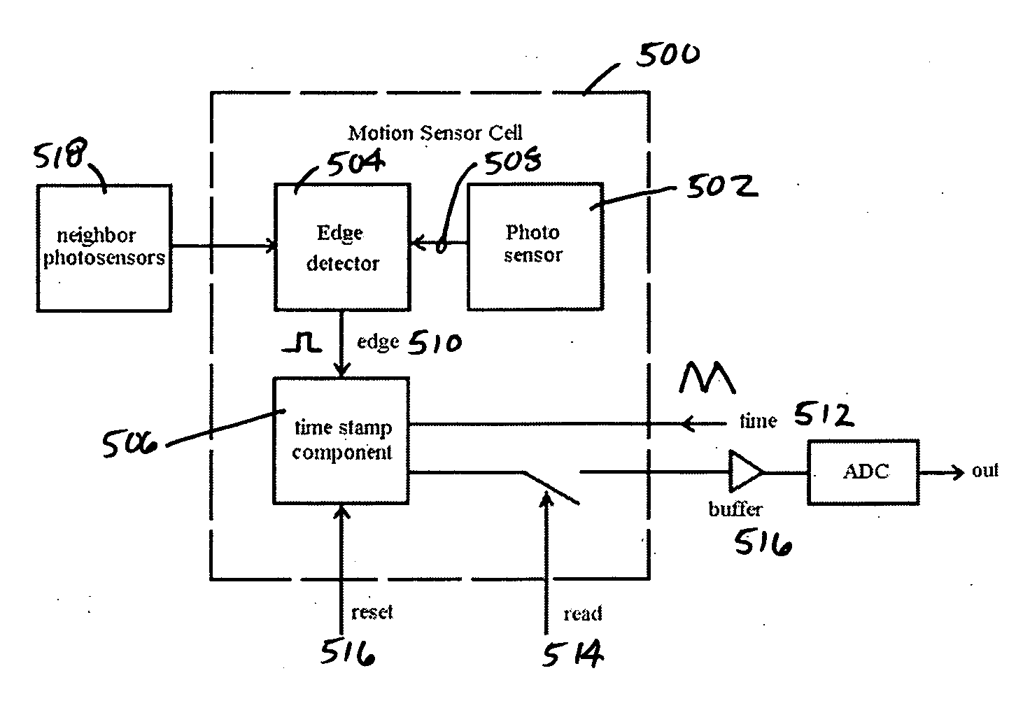
[0061] The present invention provides a method, system and apparatus for a time stamped visual motion sensor that provides a compact pixel size, higher speed motion detection and accuracy in velocity computation, high resolution, low power integration and reduces the data transfer and computation load of the following digital processor. More specifically, the present invention provides a new pixel structure based on a time stamped architecture for high-speed motion detection that solves many of the problems found in prior art devices. The relatively simple stru...


PUM

PropertyMeasurementUnit
sizeaaaaaaaaaa
pixel sizeaaaaaaaaaa
peak time resolutionaaaaaaaaaa

Abstract

The present invention provides a method, system and apparatus for a time stamped visual motion sensor that provides a compact pixel size, higher speed motion detection and accuracy in velocity computation, high resolution, low power integration and reduces the data transfer and computation load of the following digital processor. The present invention provides a visual motion sensor cell that includes a photosensor, an edge detector connected to the photosensor and a time stamp component connected to the edge detector. The edge detector receives inputs from the photosensor and generates a pulse when a moving edge is detected. The time stamp component tracks a time signal and samples a time voltage when the moving edge is detected. The sampled time voltage can be stored until the sampled time voltage is read. In addition, the edge detector can be connected to one or more neighboring photosensors to improve sensitivity and robustness.

Description

FIELD OF THE INVENTION [0001] The present invention relates generally to the field of visual motion detection, and more particularly to a method, system and apparatus for a time stamped visual motion sensor. BACKGROUND OF THE INVENTION [0002] Visual motion information is very useful in many applications such as high speed motion analysis, moving object tracking, automatic navigation control for vehicles and aircrafts, intelligent robot motion control, and real-time motion estimation for MPEG video compression. Traditional solutions use a digital camera plus digital processor or computer system. The digital camera captures the video frame by frame, transfers all the frame data to digital processor or computer and calculates the motion information using image processing algorithms, such as block matching. However, both the motion computation load and the data transfer load between the camera and the processor for large scale 2-D arrays are very high. [0003] For example, a MPEG4 CIF re...

Claims


Application Information

Patent Timeline
Patent Type & Authority Applications(United States)
IPC IPC(8): G08B13/18C12Q1/68G06M7/00G08B21/00G06K9/00H04N7/18
CPCG06T7/2033G06T2200/28G06T7/246
Inventor ZHANG, GUANGBINLIU, JIN
Owner BOARD OF RGT THE UNIV OF TEXAS SYST
Why Eureka
Try Eureka