Method for electrochemical plating on semiconductor wafers

a technology of conductive films and semiconductor wafers, applied in the direction of basic electric elements, electrical apparatus, semiconductor devices, etc., can solve the problems of step-like discontinuity in the applied current waveform, prevelant interconnections comprising copper, etc., to improve overall film quality, uniform and continuous grain structure, and reduce thermal stresses within the film

Inactive Publication Date: 2006-09-28
TAIWAN SEMICON MFG CO LTD
View PDF6 Cites 16 Cited by
  • Summary
  • Abstract
  • Description
  • Claims
  • Application Information

AI Technical Summary

Benefits of technology

[0009] As a result of the gradual increase of the current between successive stages, a more uniform and continuous grain structure is achieved througho

Problems solved by technology

However, as component sizes become smaller and more layers of metallization are fabricated, interconnections comprising copper are becoming more prevelant.
Copper interconnect electrodeposition faces a number of challenges in the form of non-uniformity of the copper layer over the wafer and filling small, high aspect ratio contactless without void formation.
The electrical current is switched almost instantly from one level to another as one stage is f

Method used


Image

  • Method for electrochemical plating on semiconductor wafers
  • Method for electrochemical plating on semiconductor wafers
  • Method for electrochemical plating on semiconductor wafers

Examples


Embodiment Construction

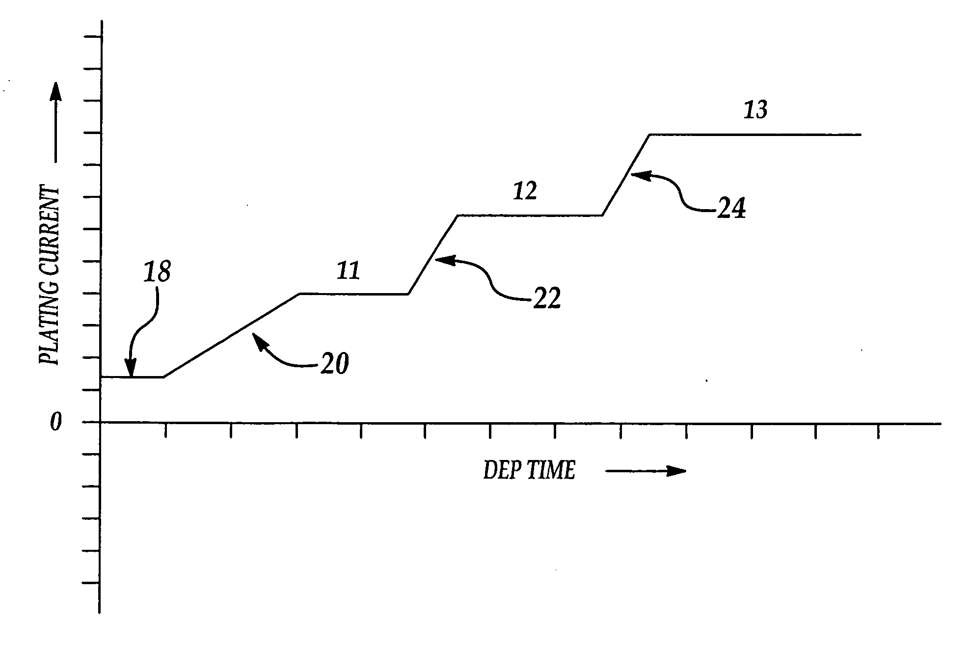
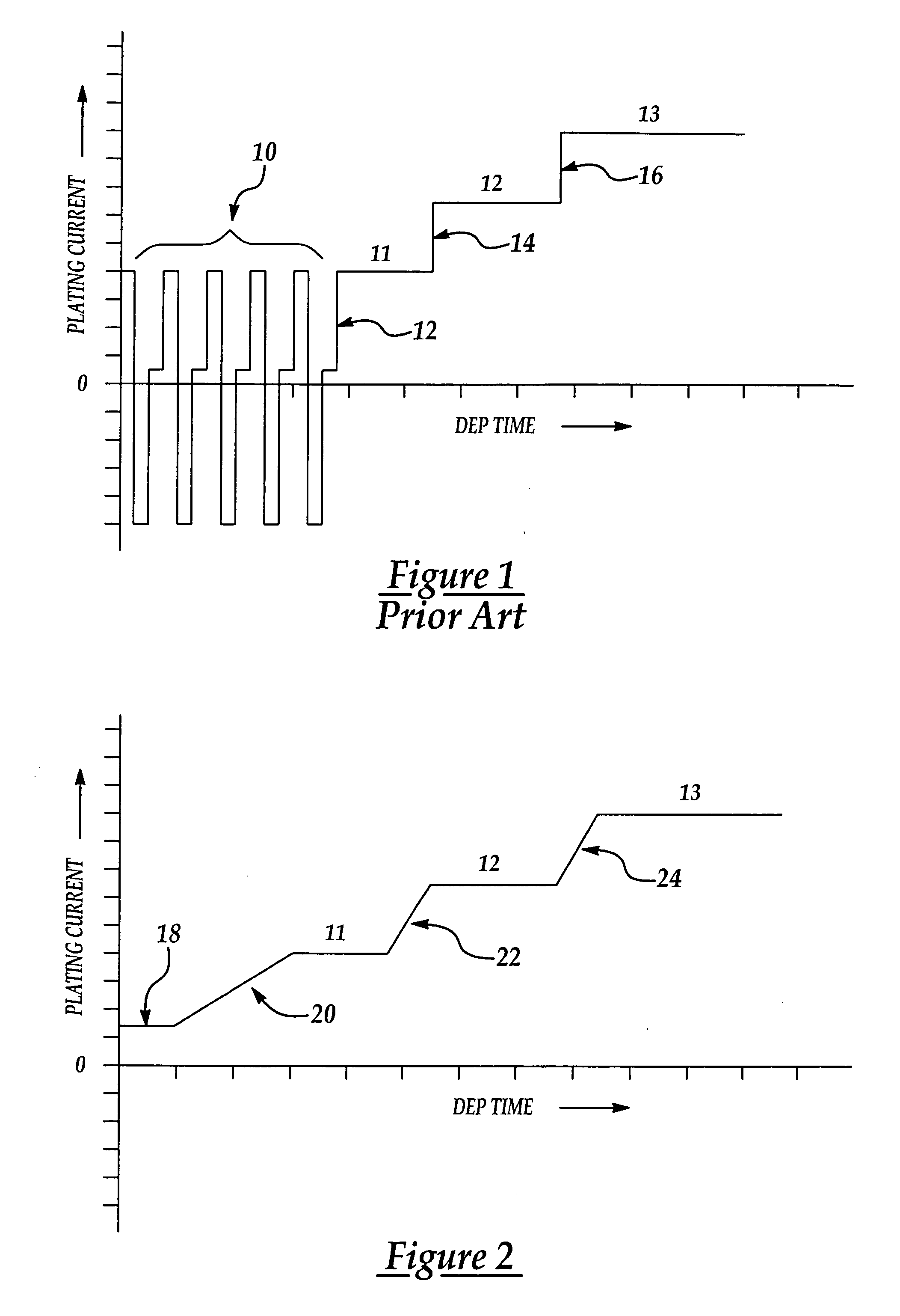
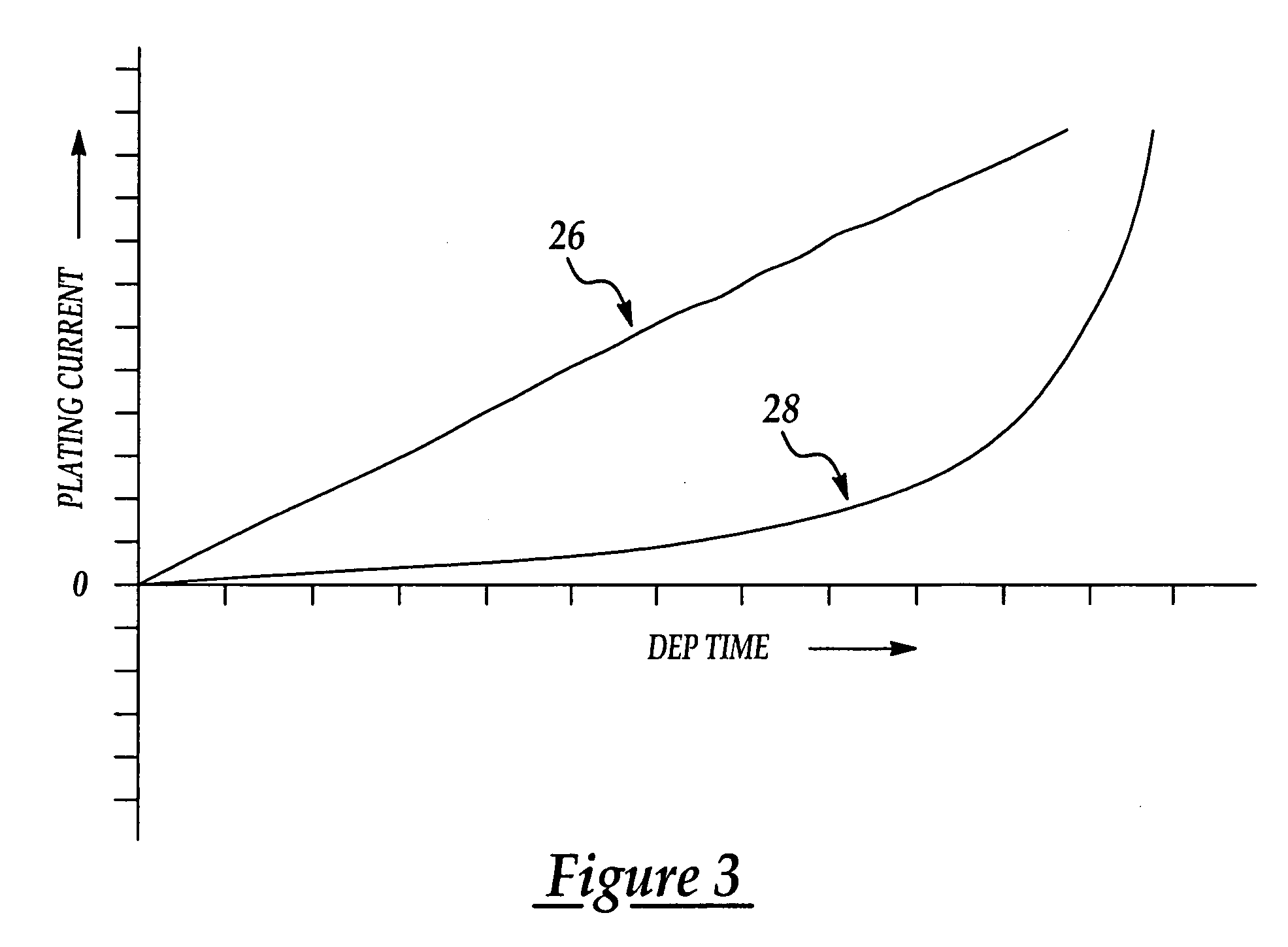
[0014] Referring first to FIG. 1, a typical process for electroplating copper on a semiconductor wafer began with depositing a barrier layer of a material such as tantalum nitride by means of sputtering. Next, a seed layer of copper is applied over the barrier layer using, for example, atomic layer deposition techniques. The seed layer of copper is applied to assure good electrical contact and adhesion of subsequent layers of copper. The seed layer of copper may be between 100 and 1000 angstroms, for example. Copper electroplating is then performed using a conventional electroplating apparatus which includes a vessel (not shown) containing an aqueous solution of CuSO4 and H2SO4, in the presence of various additives and leveling agents. The wafer is held by flexibly mounted gripping fingers (not shown) on the bottom of a spinning clam shell support which rotates the wafer while submerged within the plating bath. The wafer is electrically connected to a power source and acts as a cath...


PUM


Abstract

A method of electroplating conductive material on semiconductor wafers improves deposited film quality by providing greater control over the formation of the film grain structure. Better grain size control is achieved by applying a continuous DC plating current to the wafer which avoids sharp discontinuities in the current as the applied current is increased in successive stages during a plating cycle. Current discontinuities are avoided by gradually increasing the current in a ramp-like fashion between the successive plating stages.

Description

FIELD OF THE INVENTION [0001] This invention generally relates to electrodeposition of conductive films on semiconductor wafers, and deals more particularly with an improved method of controlling the electroplating current in order to better control grain size and improve film quality. BACKGROUND OF THE INVENTION [0002] Many typical phototolithographic integrated circuit chip fabrication processes include a deposition phase in which material of different electrical characteristics is deposited in a space created in a diffusion material. Deposition phases of lithographic processes are often utilized to create components such as resistors, diodes and transistors, and electrical interconnections between components. Current technology electrical connections often include lines and plugs that are deposited in dielectric layers of the wafer. In the past, lines typically comprised aluminum, or an aluminum alloy, and plugs included tungsten. However, as component sizes become smaller and mo...

Claims


Application Information

Patent Timeline
IPC IPC(8): C25D5/18C25D5/02
CPCC25D5/02C25D5/18H01L21/2885C25D7/123C25D5/617
Inventor CHENG, HSI-KUEILIN, STEVENHUANG, CHIH-CHANGLIAO, TZU-LINGPENG, HSIEN-PINGCHENG, MING-YUANLU, YING-JINGWANG, CHIEH-TSAOCHUANG, RAYFAN, CHEN-PENG
Owner TAIWAN SEMICON MFG CO LTD
Why Eureka
Try Eureka