Semiconductor integrated circuit device and vehicle-mounted radar system using the same

a technology of integrated circuit and semiconductor, which is applied in the direction of semiconductor devices, semiconductor/solid-state device details, instruments, etc., can solve the problems of reducing the permittivity of the substrate, reducing the insertion loss of the protection circuit, and reducing the chip area. , to achieve the effect of reducing the high-frequency loss

Active Publication Date: 2006-10-12
PANASONIC CORP
View PDF4 Cites 57 Cited by
  • Summary
  • Abstract
  • Description
  • Claims
  • Application Information

AI Technical Summary

Benefits of technology

[0023] The present invention is made in view of the above conventional problems, and its object is to provide a semiconductor integrated circuit device which includes an active circuit and a passive circuit and while permitting reduction in the chip area, can reduce the high-frequency loss and prevent an interconnect from being partly removed at the bend.
[0026] According to the semiconductor integrated circuit device of the present invention, since the Group III-V nitride semiconductor layer forming the active circuit is formed on part of the insulative substrate, this eliminates the need for forming an isolation region in a nitride semiconductor layer having conductivity. This can reduce the chip area without resistance variations, for example, in the increase of the resistance of the nitride semiconductor layer for the formation of the isolation region using ion implantation. Furthermore, since the passive circuit is formed with the dielectric film interposed between the substrate and the passive circuit, this can suppress the loss of an RF signal due to an interconnect. Moreover, since the first interconnect is formed on the dielectric film formed to cover the top and side surfaces and upper corners of the Group III-V nitride semiconductor layer, the first interconnect can be prevented from being partly removed.
[0030] It is preferable that the semiconductor integrated circuit device of the present invention further comprises: a conductive film formed on the surface of the substrate opposite to the passive circuit; and a second interconnect through which the passive circuit and the conductive film are electrically connected to each other, said second interconnect being formed to pass through the substrate. This allows continuity through the second interconnect between the passive circuit and the conductive film formed on the back surface of the substrate. Therefore, the parasitic inductance due to an interconnect can be minimized.
[0031] It is preferable that the semiconductor integrated circuit device of the present invention filer comprises a bump formed on part of the dielectric film and electrically connected to the passive circuit. This can provide a so-called flip-chip packaging in which the active circuit and the passive circuit are opposed to each other on a mounting member for packaging. This eliminates the need for electrically connecting the active circuit to the passive circuit by wire bonding. Therefore, the use of flip-chip packaging can reduce the chip area and also the high frequency loss caused by bonding wires.

Problems solved by technology

Therefore, it becomes unnecessary for each of GaN-based low-noise devices forming a reception circuit to have an input protection circuit that has been required to cope with an external surge, resulting in the reduced insertion loss of the protection circuit.
Furthermore, input power can be set high such that an interference wave produced at the output side with increase in an input signal becomes ignorable and the voltage of the input power does not exceed the breakdown voltage of the GaN-based low-noise device.
Furthermore, when the insulation performance of a substrate that determines high-frequency characteristics is not uniform, this reduces the permittivity of the substrate as compared with the case where a substrate is uniformly insulated.
As a result, the area of an MMIC chip is increased, leading to problems in downscaling the chip.
The increase in the area of the chip becomes one of factors responsible for the increased cost.

Method used


Image

  • Semiconductor integrated circuit device and vehicle-mounted radar system using the same
  • Semiconductor integrated circuit device and vehicle-mounted radar system using the same
  • Semiconductor integrated circuit device and vehicle-mounted radar system using the same

Examples


embodiment 1

[0044] A first embodiment of the present invention will be described with reference to the drawings.

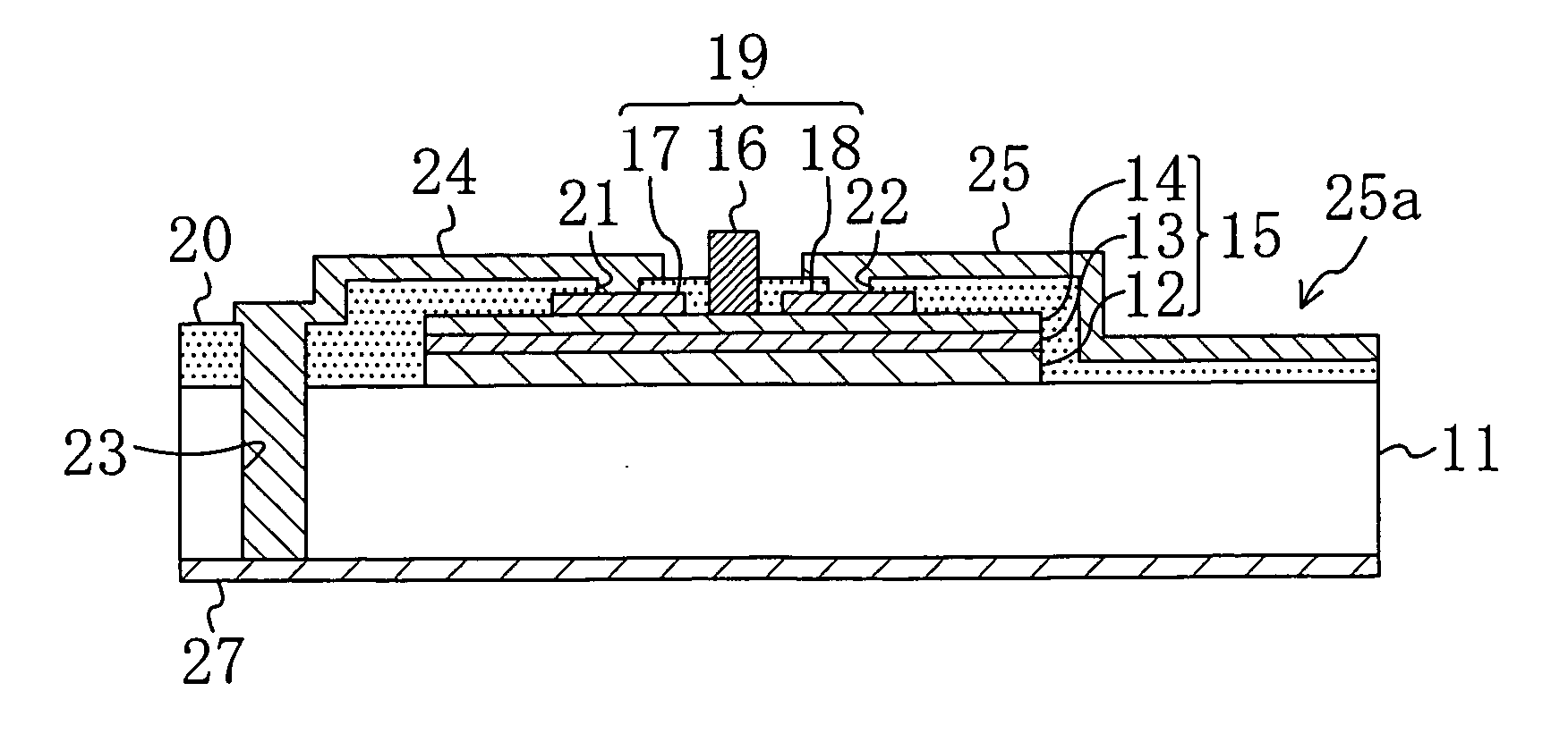
[0045]FIGS. 1A and 1B show a semiconductor integrated circuit device according to the first embodiment of the present invention. FIG. 1A is a plan view of a microwave or millimeter-wave MMIC including a GaN-based HFET serving as an active circuit and a microstrip line serving as a passive circuit. FIG. 1B is a cross-sectional view taken along the line 1b-1b in FIG. 1A. The structure of the MMIC and a fabrication method for the MMIC will be described hereinafter.

[0046] First, a 0.5-μm-thick buffer layer 12 made of undoped aluminum nitride (AlN), a 3-μm-thick channel layer 13 made of undoped gallium nitride (GaN), through which carriers travel, and a 25-nm-thick carrier supplying layer 14 made of n-type aluminum gallium nitride (AlGaN) are successively grown, by MOVPE, on the principal surface of an insulative substrate 11, for example, made of sapphire. In this way, a Group III-V nit...

embodiment 2

[0078] A second embodiment of the present invention will be described hereinafter with reference to the drawings.

[0079]FIGS. 4A and 4B show a semiconductor integrated circuit device according to the second embodiment of the present invention. FIG. 4A is a plan view of a microwave or millimeter-wave MMIC including a GaN-based HFET serving as an active circuit and a MIM (metal-insulator-metal) capacitor serving as a passive circuit. FIG. 4B is a cross-sectional view taken along the line IVb-IVb in FIG. 4A. In FIGS. 4A and 4B, the same reference numerals are given to the same components as shown in FIGS. 1A, 1B, 3A, and 3B, and a description of these components is not given.

[0080] As shown in FIGS. 4A and 4B, a MIM capacitor 44 is formed on part of the principal surface of a substrate 11 of sapphire located closer to a drain electrode 18 of a HFET 19 with a first dielectric film 30 interposed between the substrate 11 and the MIM capacitor 44. The MIM capacitor 44 is composed of a low...

embodiment 3

[0093] A third embodiment of the present invention will be described hereinafter with reference to the drawings.

[0094] As described in the background of the invention, a transistor or diode element using gallium nitride (GaN) having a relatively large band gap of 3.39 eV achieves a higher breakdown voltage, a higher-temperature operation, a higher resistance to a surge voltage, higher power handling, and lower distortion (lower intermodulation distortion) than that using gallium arsenic (GaAs). Furthermore, the on-resistance of the GaN-based transistor or diode element during the operation thereof is lower than that of the GaAs-based transistor or diode element, leading to low-noise characteristics.

[0095] In view of the above, GaN-based devices are suitable as basic devices forming RF front-end sections of radio communication systems or radar systems.

[0096]FIG. 5 is a block diagram showing an exemplary RF front-end section of a vehicle-mounted radar system using a pulse radar met...


PUM


Abstract

A semiconductor integrated circuit device includes a HFET formed on part of a substrate made of sapphire and including a Group III-V nitride semiconductor layer, a dielectric film formed on the substrate to cover the top and side surfaces and upper corners of the Group III-V nitride semiconductor layer, a microstrip line formed with the dielectric film interposed between the substrate and the microstrip line, and a drain lead which is formed on part of the dielectric film and through which the HFET is electrically connected to the microstrip line.

Description

CROSS-REFERENCE TO RELATED APPLICATIONS [0001] The disclosure of Japanese Patent Application No. 2004-337112 filed on Nov. 22, 2004 and Japanese Patent Application No. 2005-336104 filed on Nov. 21, 2005 including specification, drawings and claims is incorporated herein by reference in its entirety. BACKGROUND OF THE INVENTION [0002] (1) Field of the Invention [0003] The present invention relates to a semiconductor integrated circuit device and a vehicle-mounted radar system using the same, and more particularly relates to a monolithic microwave integrated circuit (MMIC) device in which an active circuit and a passive circuit are monolithically integrated. [0004] (2) Description of Related Art [0005] High-frequency parts used for mobile communication systems typified by cellular phones or vehicle-mounted radar systems have been demanded to have improved performance and a reduced size. [0006] Conventionally, field-effect transistors (FETs) or heterostructure field-effect transistors ...

Claims


Application Information

Patent Timeline
Patent Type & Authority Applications(United States)
IPC IPC(8): H01L29/06
CPCG01S7/032H01L2924/01033H01L23/66H01L24/24H01L24/82H01L29/2003H01L29/7787H01L2223/6627H01L2224/24011H01L2224/24051H01L2924/01005H01L2924/01013H01L2924/01029H01L2924/01032H01L2924/01078H01L2924/01079H01L2924/01082H01L2924/10329H01L2924/14H01L2924/1423H01L2924/1903H01L2924/19041H01L2924/19042H01L2924/19043H01L2924/19105H01L2924/30105H01L2924/30107H01L2924/3011H01L2924/01006H01L2924/01023H01L23/481H01L2924/12032H01L2924/00
Inventor NISHIJIMA, MASAAKIUEDA, DAISUKE
Owner PANASONIC CORP
Why Eureka
Try Eureka