Polishing composition and polishing method

a technology of polishing composition and polishing method, which is applied in the direction of lapping machines, manufacturing tools, other chemical processes, etc., can solve the problems of difficult cu formation, difficult lapping, and increased irregularities, and achieves excellent electrical characteristics, good polishing effect, and low cost.

Inactive Publication Date: 2007-01-04
ASAHI GLASS CO LTD +1
View PDF6 Cites 14 Cited by
  • Summary
  • Abstract
  • Description
  • Claims
  • Application Information

AI Technical Summary

Benefits of technology

[0027] According to the present invention, in polishing a surface to be polished in the production of a semiconductor integrated circuit device, it is possible to form an embedded wiring portion with few scratches, high reliability and excellent electrical characteristics while dishing or erosion is suppressed, by preferentially polishing a convex portion while suppressing preferential polishing of a concave portion, at a high removal rate.

Problems solved by technology

That is, as the multilayered wirings are increasingly formed due to the miniaturization and densification in the semiconductor production processes, the degree of irregularities tends to increase in the surfaces of the individual layers, resulting in a situation where the step height exceeds the depth of focus in lithography.
Since the vapor pressure of copper chloride gas is low, it is difficult to form Cu into the shape of wirings by Reactive Ion Etching (RIE) which has been conventionally used.
However, since the barrier layer is significantly harder than Cu, it is often not possible to achieve a sufficient removal rate.
Thus, the planarization is carried out by polishing, but in CMP using the conventional polishing composition, an increase in dishing and erosion in the Cu-embedded wirings 6 will give rise to problems.
Furthermore, the polishing pressure applied to the barrier layer 3 and the insulating layer 2 therebeneath in a highly dense wiring portion becomes relatively greater than that applied to a less dense wiring portion, so that the removal rate in the second polishing step largely differs depending on the wiring density, and as a result, the insulating layer 2 in the highly dense wiring portion is over-polished, resulting in a large extent of erosion.
When such dishing or erosion occurs, the wiring resistance tends to increase and electromigration tends to readily occur, resulting in the reduction of the reliability of devices.
Tantalum and tantalum compounds to be used for the barrier layer are difficult to be etched chemically.
Because of their higher hardness than Cu, tantalum and tantalum compounds are difficult to be removed mechanically by polishing.
If abrasive particles with a higher hardness are used in order to increase the removal rate, scratches will occur in the soft Cu wirings, resulting in problems such as electrical defects.
If the concentration of abrasive particles in the polishing composition is increased, it becomes difficult to maintain the dispersion of the abrasive particles in the polishing composition, and problems are likely to occur in the dispersion stability, such as sedimentation and gelation with time.
However, there has been a problem such that if it is attempted to cope with dishing only by increasing the amount of BTA, the removal rate of Cu lowers, and the removal time becomes long, whereby defects of dishing and erosion may sometimes increase.
However, the thickness of the barrier layer is usually thin at a level of from 20 to 40 nm, and further, Cu is polished and removed at a high speed in the first polishing step, and therefore, it is extremely difficult to suppress dishing to be thinner than the thickness of the barrier layer.
Further, in a case where there is a distribution in the Cu removal rate in the first polishing step, it is required to carry out over-polishing to completely remove unnecessary Cu residue in the wafer, whereby it tends to be more difficult to suppress dishing to a low level.
In recent years, as the generation of semiconductor advances and the wiring portion becomes thinner, reduction of such erosion has been a serious problem to be solved.

Method used


Image

  • Polishing composition and polishing method
  • Polishing composition and polishing method
  • Polishing composition and polishing method

Examples


examples

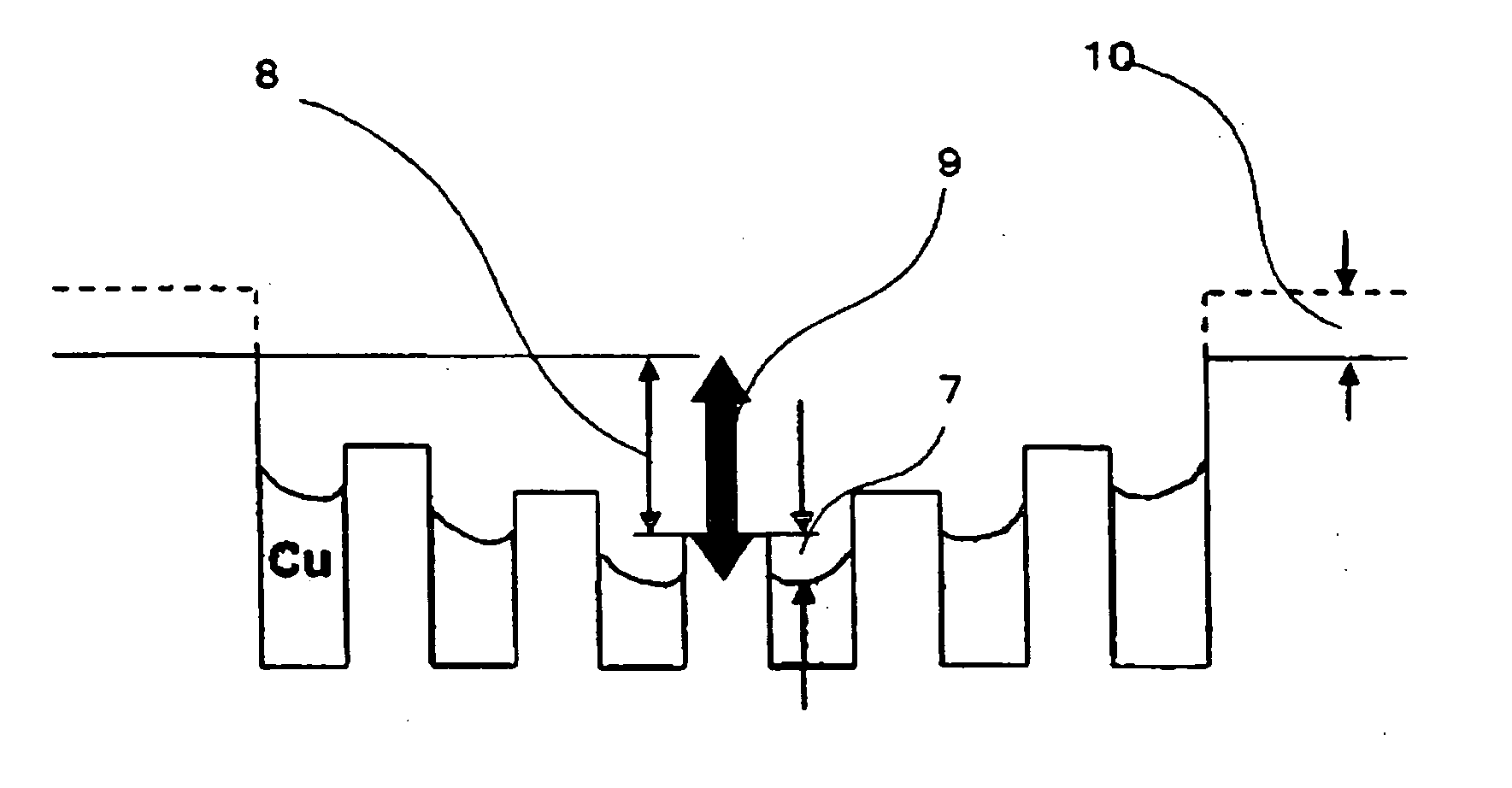
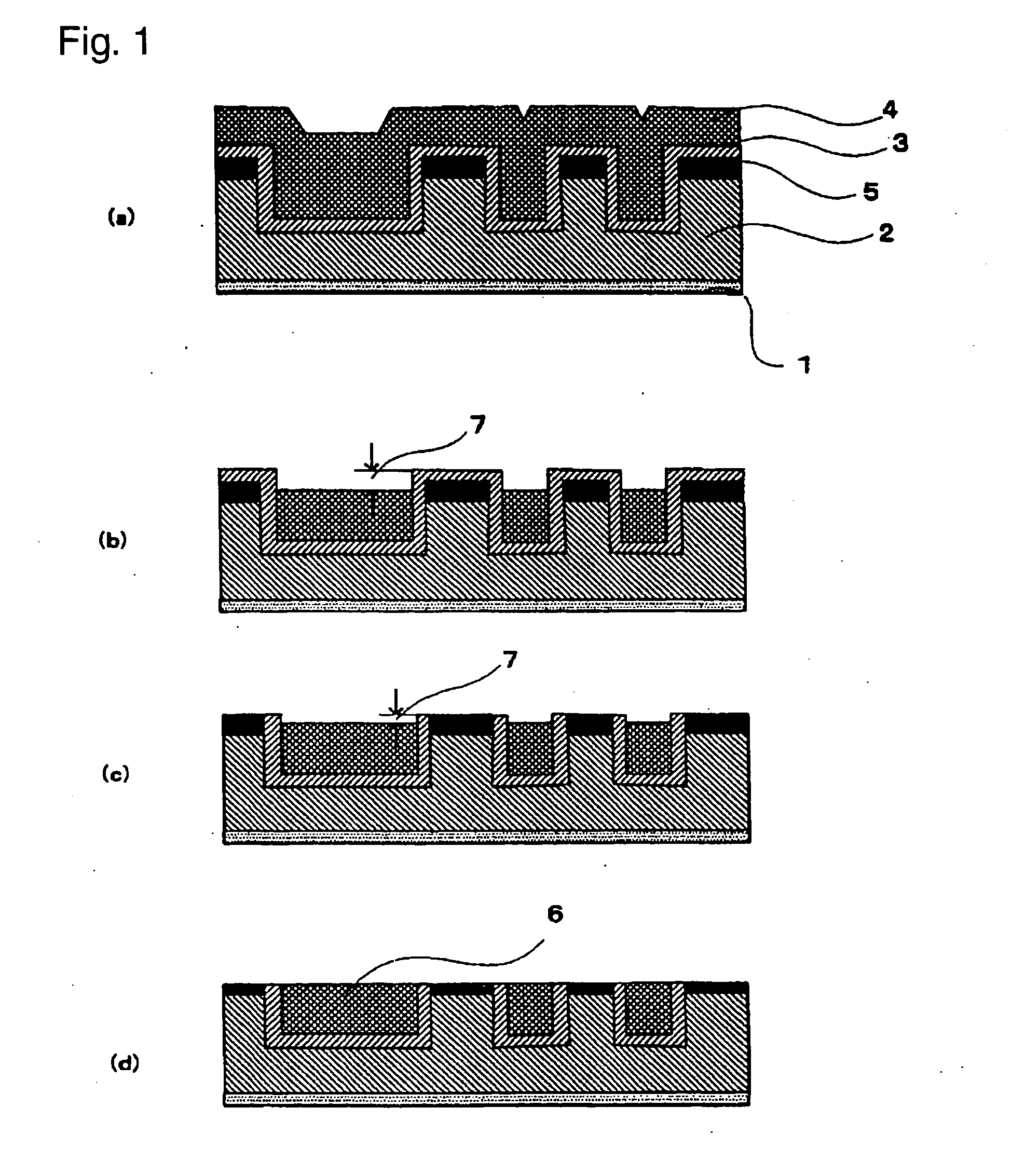
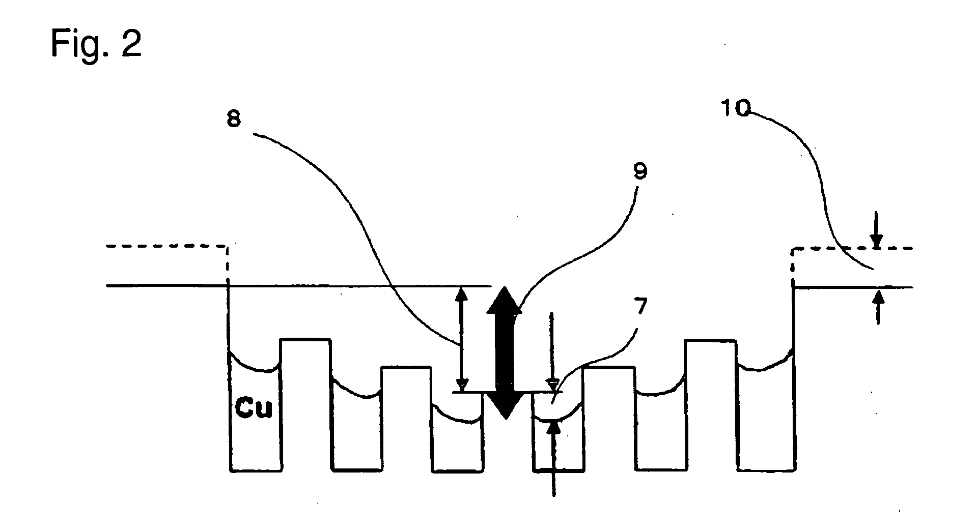
[0074] Now, the present invention will be described in further detail with reference to Examples of the present invention (Examples 1 to 3, and Examples 8 to 12) and Comparative Examples (Examples 4 to 7).

(1) Preparation of Polishing Composition

[0075] Each polishing composition in Examples 1 to 7 was prepared as follows. An acid, a basic compound and a pH buffering agent were added to water, followed by stirring for 10 minutes to obtain liquid a. Then, the component (E) was dissolved in ethylene glycol so that the solid content concentration would be 40 mass %, and the resultant was added to liquid a. Then, the component (B) was further added thereto, followed by stirring for 10 minutes to obtain liquid b.

[0076] Then, an aqueous dispersion of the component (A) was slowly added to the liquid b, and then a basic compound was slowly added thereto to adjust the pH to 3. An aqueous solution of the component (D) was further added thereto, followed by stirring for 30 minutes, to obtain...


PUM

PropertyMeasurementUnit
thicknessaaaaaaaaaa
mean particle diameteraaaaaaaaaa

Abstract

To provide a polishing composition which has a high removal rate and enables to suppress occurrence of dishing and erosion, in polishing of a surface to be polished in the production of a semiconductor integrated circuit device. A chemical mechanical polishing composition for polishing a surface to be polished of a semiconductor integrated circuit device comprises (A) fine oxide particles, (B) pullulan, and (C) water. The polishing composition further contains (D) an oxidizing agent, and (E) a compound represented by the formula 1: wherein R is a hydrogen atom, a C1-4 alkyl group, a C1-4 alkoxy group or a carboxylic acid group.

Description

TECHNICAL FIELD [0001] The present invention relates to a polishing composition to be used in a process for producing a semiconductor device. More particularly, it relates to a polishing composition which is suitable for forming an embedded metal wiring in which a Cu-based metal is used as a material for wirings and a tantalum-based metal is used as a material for barrier layers, and a method for polishing a surface to be polished of a semiconductor integrated circuit device using the polishing composition. BACKGROUND ART [0002] Recently, as the integration and functionality of semiconductor integrated circuits have been increasing, there has been a demand for development of micro-fabrication techniques for miniaturization and densification. Planarization techniques for interlayer insulating films and embedded wirings are important in semiconductor device production processes, in particular, in the process of forming multilayered wirings. That is, as the multilayered wirings are inc...

Claims


Application Information

Patent Timeline
Patent Type & Authority Applications(United States)
IPC IPC(8): H01L21/44H01L21/461B24B37/00C09K3/14H01L21/304H01L21/3105H01L21/321
CPCB24B37/044H01L21/3212H01L21/31053C09K3/1463H01L21/304
Inventor TAKEMIYA, SATOSHISHINMARU, SACHIE
Owner ASAHI GLASS CO LTD
Why Eureka
Try Eureka