Apparatus for aberration detection and measurement

a technology of aberration detection and measurement apparatus, applied in the field of microlithographic imaging, can solve the problems of inconvenient microlithographic application of rayleigh /4 rule, dependant on reference beam (and reference wave error), field use (or in-situ application), etc., and achieve the effect of easing the distinction of aberrations

Inactive Publication Date: 2007-01-25
SMITH BRUCE W
View PDF14 Cites 63 Cited by
  • Summary
  • Abstract
  • Description
  • Claims
  • Application Information

AI Technical Summary

Problems solved by technology

This Rayleigh λ / 4 rule is not suitable however for microlithographic applications.
A more significant limitation of these interferometric methods in the need for the reference and test beams to follow separated paths, making field use (or in-situ application) difficult.
This is the main difficulty with employing these methods for in-situ measurement on a lithography tool.
The two primary sources of error with these methods are systematic geometric effects that arise from the geometry of the system (which can be compensated for if measurable) and imperfections in the pinhole.
Pinhole imperfections result in reference beam (and reference wave) error dependant on the size, shape, and positioning of the pinhole.
There is a real limitation to the fluence that can pass though a pinhole and the fabrication capabilities required to make such an artifact.
Large numerical apertures will also make image capture difficult and secondary optical relay systems may be required.
Although PSPD methods have a good deal of potential for accurate wavefront measurement, implementation will likely be difficult without modifications to stepper or scanner hardware.
Various enhancements to this approach have proven capability at the levels needed for microlithography application but implementation may be difficult.
A major limitation to these types of tests is that the test is insensitive to small wavefront slope changes, in terms of either magnitude or direction.
In other words, when the first or second derivatives of the wavefront errors are small, these tests are quite insensitive.
This is especially problematic with large apertures.
The problem with this method is its qualitative aspect.
This may prove difficult, however, since diffraction limited pinhole images would be difficult to record with any detail in photoresist.
These methods are limited, however, by the requirement of a reflective optical system.
Practical application for microlithographic purposes is therefore also limited.
Fabrication of this reticle becomes challenging then as a range of etch angles must be accommodated.
This becomes challenging with current exposure tools that limit sigma to values above 0.3.
Lower values will result in significant loss in image intensity.
This implies that the resists used for IC fabrication would not be well suited and special materials and modifications to processes would most likely be required.
This is challenging for partially coherent imaging but correlation approaches exist.
Two difficulties arise with this method of image assessment for optical lithography.
First is the problem with the separating of aberration types and understanding their contribution to losses in the spread or transfer functions.
Small levels of aberration can have similar impact and identification of azimuthal orders will be difficult.
The second set of challenges with this method comes with making the mask and detector artifacts that are small enough to give the resolution required for images of interest, accurately producing arrays of these features at the detector, and getting sufficient energy though a small “pinhole” or slit feature.
The phase shift focus monitor approach is very useful for fitting low order aberration but discrimination over a given azimuthal term is difficult.
Complete description of an aberrated wavefront is difficult.
This method is adequate for the detection of comatic aberration but it is difficult to extract the magnitude of such aberrations or the presence of other aberrations.
One problem screen type methods inherently possess is the inability to detect small scale surface changes taking place between the holes in the screen.
Additional challenges encountered with screen tests include methods of data collection and data reduction.
A fundamental problem with screen tests is the inability to test wavefront positions between those tested with the screen openings
As partial coherence is decreased, however, less of the full lens pupil is utilized to image the phase edge and correlation to full wavefront information is difficult.
This complicates the process to some degree by requiring multiple exposure and measurement passes.
The extraction and interpretation of aberrations from the images is often difficult and time consuming because of the often subtle shape deformation that is introduced into the ring images with low and moderate levels of aberration.
Large amounts of data are often needed for conclusive results.
Consequently, the method is often only practiced by individuals that are well trained in the fitting and interpretation of the ring image results.

Method used


Image

  • Apparatus for aberration detection and measurement
  • Apparatus for aberration detection and measurement
  • Apparatus for aberration detection and measurement

Examples


Embodiment Construction

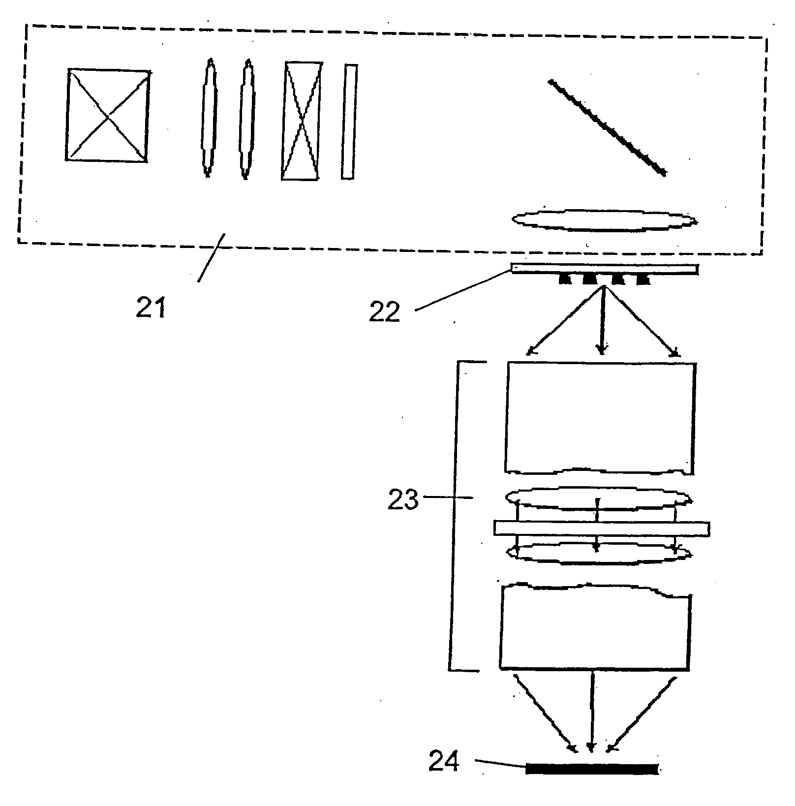
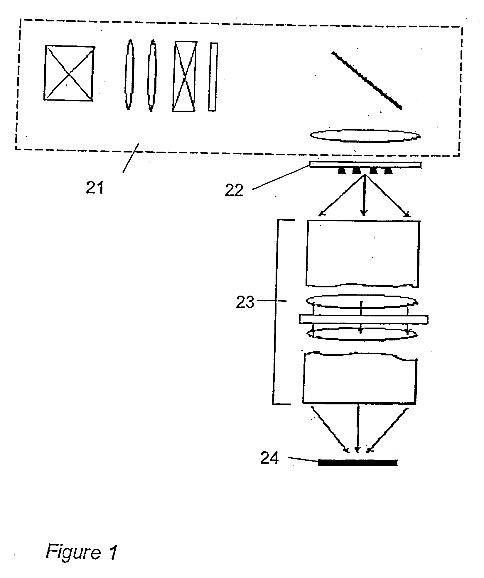
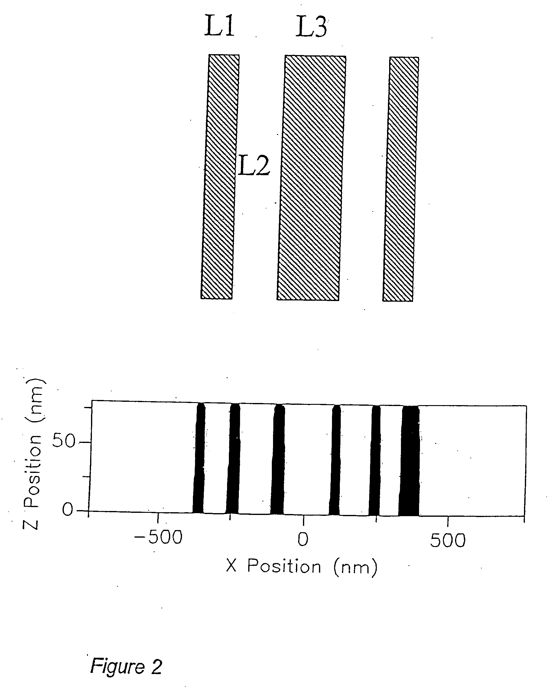
[0053] When imaging with a projection optical system, the aberrations in the lens pupil introduce deformation to a wavefront resulting in imaging errors. FIG. 1 shows a schematic of a projection imaging system. An illumination apparatus 21 illuminates a mask test object 22 which is imaged through an objective lens 23 onto a photosensitized substrate 24. If a test object is employed on a photomask as a phase pattern, specifically with a phase shifted from that of the surrounding area by 180 degrees, the lens aberration will introduce imaging errors characteristic of the aberration type and the mask geometry. As an example, FIG. 2 shows how three small phase lines (between 0.5 and 1.5 lambda / NA) are printed into a photoresist. The images are a result of lithographic simulation using a Prolith vector model (Prolith Version 7.0, KLA FINLE) with a wavelength of 157 nm, a numerical aperture (NA) of 0.85, a partial coherence value of 0.30, and a resist thickness of 80 nm. The resulting ima...


PUM

PropertyMeasurementUnit
wavelengthsaaaaaaaaaa
anglesaaaaaaaaaa
thicknessaaaaaaaaaa

Abstract

Aberrations in an optical system can be detected and measured using a method comprised of a test target in the object plane of a projection system and imaging a photoresist film with the system. The test target comprises at least one open figure which comprises a multiple component array of phase zones, where the multiple zones are arranged within the open figure so that their response to lens aberration is interrelated and the zones respond uniquely to specific aberrations depending on their location within the figure. This is a unique and new method of detecting a variety of aberration types including coma, spherical, astigmatism, and three-point through the exposure of a photoresist material placed in the image plane of the system and the evaluation of these images.

Description

CROSS REFERENCE TO RELATED APPLICATIONS [0001] This application is a Divisional of U.S. patent application Ser. No. 10 / 734,462 filed Dec. 12, 2003, which claims the benefit of the priority date of U.S. Provisional Patent Application Ser. No. 60 / 433,153 filed Dec. 13, 2002.FIELD OF THE INVENTION [0002] The present invention relates to microlithographic imaging using a projection exposure system for fabricating semiconductor devices and the detection of aberrations in the system BACKGROUND OF THE INVENTION [0003] Optical lithography has been the dominant technology for the patterning of semiconductor device features. As the size of the geometry for these devices continue to shrink below the ultraviolet (UV) wavelength used for imaging, significant demands are placed on the quality of the optical component within the projection imaging system. The projection system used for imaging of sub-wavelength features coprise a large number of lens elements and operate at wavelengths ranging fro...

Claims


Application Information

Patent Timeline
Patent Type & Authority Applications(United States)
IPC IPC(8): G03B27/68G01M11/02G03F7/20
CPCG03F7/706G01M11/0264
Inventor SMITH, BRUCE W.
Owner SMITH BRUCE W
Why Eureka
Try Eureka