Method for manufacturing semiconductor device

a manufacturing method and semiconductor technology, applied in semiconductor devices, chemical vapor deposition coatings, coatings, etc., can solve the problems of lowering the insulating property of the film, high probability of oxygen diffusion in the film, and high interface sta

Inactive Publication Date: 2007-02-22
KK TOSHIBA
View PDF1 Cites 37 Cited by
  • Summary
  • Abstract
  • Description
  • Claims
  • Application Information

AI Technical Summary

Benefits of technology

[0036] A method for manufacturing a semiconductor device according to a first aspect of the present invention includes: forming an insulation film having at least one kind of bonds selected out of silicon-nitrogen bonds and metal-oxygen bonds on either a film having...

Problems solved by technology

If the film thickness of the insulation film becomes approximately 10 nm or less, however, the probability that electrons and holes pass through the film is increased by the tunnel effect, resulting in a lowered insulating property of the film.
If the silicon oxide film is made too thin according to device shrinkage, however, it is more likely that nitrogen diffuses to the interface between the silicon oxide film and the substrate at the time of plasma nitridation, resulting in higher interface state.
Furthermore, probability of oxygen diffusion in the film is high at places where impurities exist.
Even when plasma nitridation is performed using gas that does not contain hydrogen, such as pure nitrogen, too much decreasing of nitridation temperature reduces resistance of a silicon nitride film against oxidation.
f the island-shaped nitride film is oxidized, however, a thick oxide film is partially generated by oxygen diffused through places where the film is thin, resulting in a problem of lowered electrical characteristics of the whole dielectric film.
This is because too much raising the deposition temperature causes phase separation and crystallization of a high-k material, producing a film with uneven composition and thickness.
On the other hand, trapping of electrons and holes is apt to occur and the level of the leak current is also high, in the insulation film formed at a too low temperature.
On the other hand, it is reported that the following problems occur when a polycrystalline silicon film is used as an electrode of a high-k insulation film.
One possibility is that during deposition of polycrystalline silicon on a high-k film or heating it to activate impurities contained in the polycrystalline silicon film, the polycrystalline silicon film reacts with high-k insulation film, producing defect such as oxygen vacancy at the interface between electrode and high-k film.
Reaction between polycrystalline silicon and high-k film also induces silicon atom diffusion from electrode into a high-k film, resulting in a lowered film quality of the high-k insulation film.
Even in the case where a metal film or a metal compound is used as the electrode, a similar problem could occur depending upon the kind of the metal.
Therefore, these films contain impurity such as NHx, CHx and OH and defect to some degree.
The impurity and defect contained in the reaction suppression layer, not only lower electric characteristics but also degrades barrier property of the film.
It is difficult to remove impurity and defect completely from the film even if heat treatment at very high temperature is conducted in the conventional RTA equipment.
To form a reac...

Method used


Image

  • Method for manufacturing semiconductor device
  • Method for manufacturing semiconductor device
  • Method for manufacturing semiconductor device

Examples


first embodiment

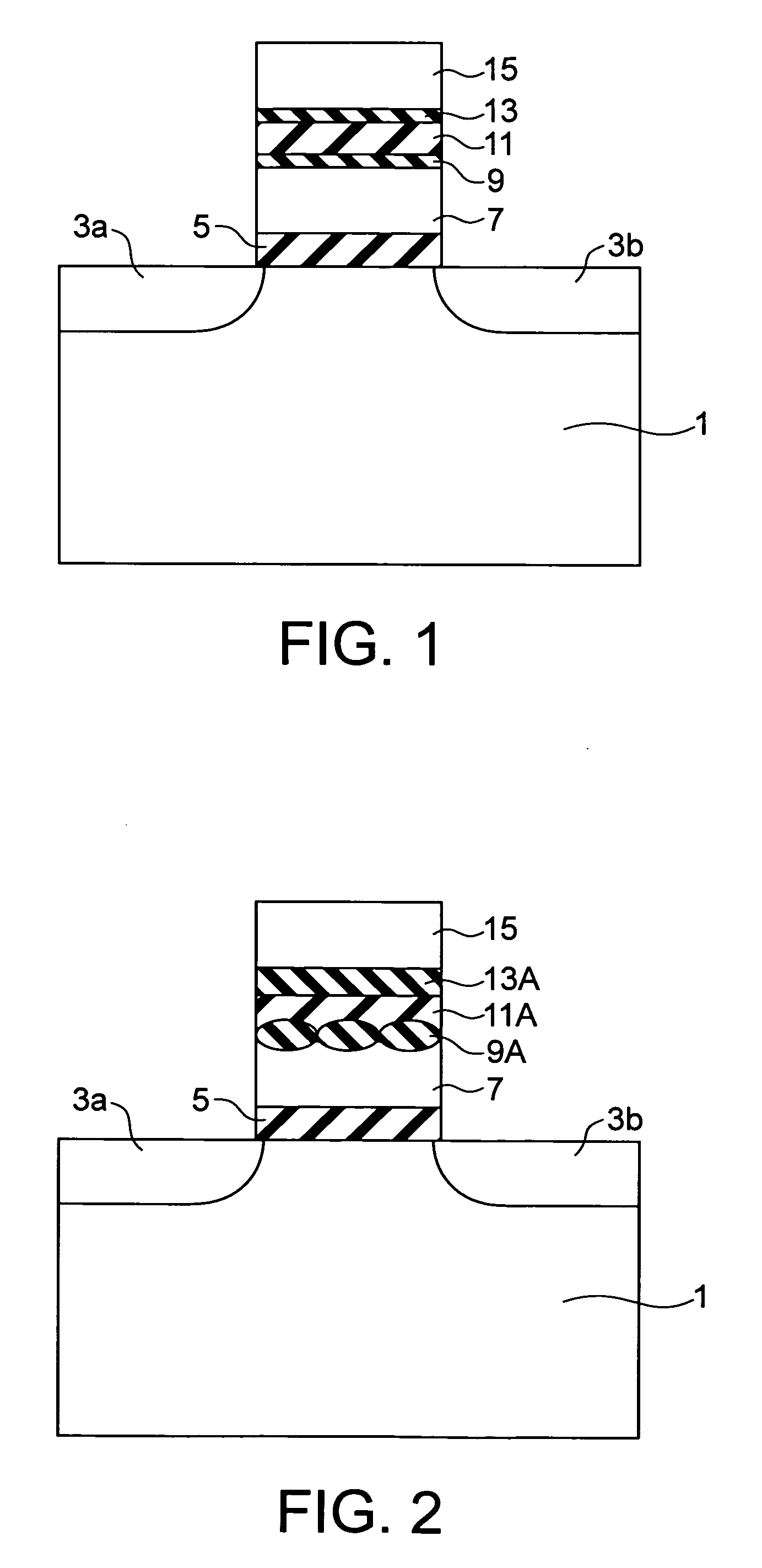
[0053] A manufacturing method of a semiconductor device according to a first embodiment of the present invention will now be described. A semiconductor device manufactured by using the manufacturing method according to the present embodiment is shown in FIG. 1. This semiconductor device is a flash memory. FIG. 1 shows a sectional view of its memory cell. In this memory cell, a source region 3a and a drain region 3b kept apart are formed on a silicon substrate 1. A tunnel oxide film 5 is formed on the silicon substrate 1 between the source region 3a and the drain region 3b. A floating electrode 7 is formed of polycrystalline silicon with phosphorus added on the tunnel oxide film 5. A lower silicon nitride film 9 is formed on the floating electrode 7. A high-k insulation film 11 is formed of HfSiO on the lower silicon nitride film 9. An upper silicon nitride film 13 is formed on the high-k insulation film 11. A control electrode 15 is formed of polycrystalline silicon with phosphorus ...

second embodiment

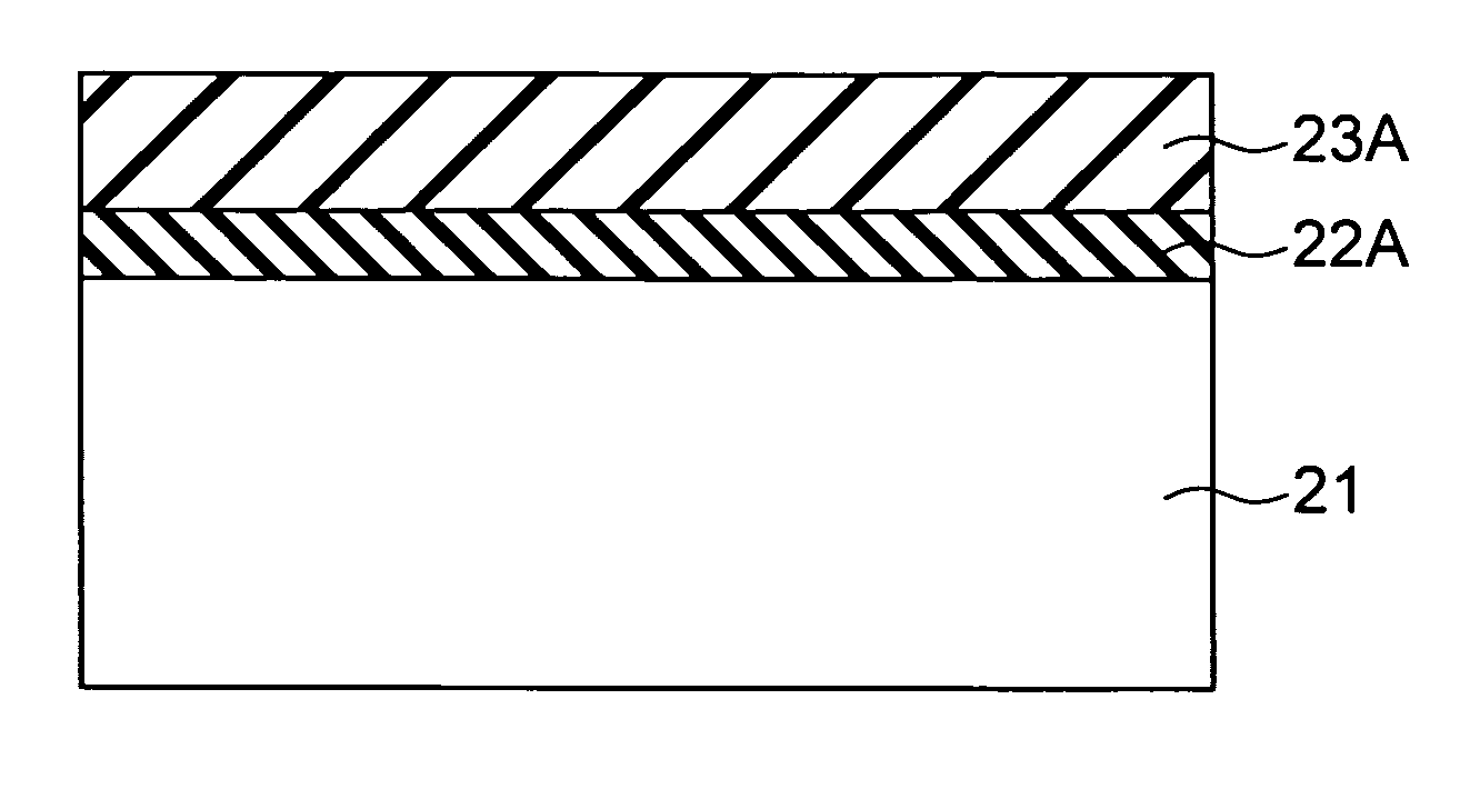
[0076] A manufacturing method of a semiconductor device according to a second embodiment of the present invention will now be described. FIG. 5 is a sectional view of a semiconductor device manufactured by using a manufacturing method according to the present embodiment. In this semiconductor device, a high-k gate insulation film 23 is formed on a silicon substrate 21. This semiconductor device is manufactured as hereafter described.

[0077] First, the silicon substrate 21 is subjected to wet cleaning, and contamination and a natural oxide film on the surface are removed. Thereafter, an HfSiO film having a thickness of approximately 5 nm is formed at approximately 600° C. by using the MOCVD method. In addition, the HfSiO film is subjected to exposure to infrared laser light having a wavelength of 8.5 μm and a pulse width of 10 fs in an atmosphere of oxygen under the atmospheric pressure in order to remove impurities and defects contained in the film. The high-k gate insulation film 2...


PUM

PropertyMeasurementUnit
Temperatureaaaaaaaaaa
Timeaaaaaaaaaa
Lengthaaaaaaaaaa

Abstract

It is made possible to form a silicon nitride film, an aluminum oxide film and a transition metal high-k insulation film of high quality. A manufacturing method includes: forming an insulation film having at least one kind of bonds selected out of silicon-nitrogen bonds, aluminum-oxygen bonds, transition metal-oxygen-silicon bonds, transition metal-oxygen-aluminum bonds, and transition metal-oxygen bonds on either a film having a semiconductor as a main component or a semiconductor substrate, and irradiating the insulation film with pulse infrared light having a wavelength corresponding to a maximum intensity in a wavelength region depending upon the insulation film and having a wavelength absorbed by the insulation film.

Description

CROSS-REFERENCE TO RELATED APPLICATION [0001] This application is based upon and claims the benefit of priority from prior Japanese Patent Application Nos. 2005-240192 and 2006-174262, filed on Aug. 22, 2005 and Jun. 23, 2006 in Japan, the entire contents of which are incorporated herein by reference. BACKGROUND OF THE INVENTION [0002] 1. Field of the Invention [0003] The present invention relates to a method for manufacturing a semiconductor device having a silicon nitride film or an aluminum oxide film having a dielectric constant greater than that of a silicon oxide, or a high-k insulation film. [0004] 2. Related Art [0005] Until now, a silicon oxide film having high insulating property generated by thermal oxidation has been used as the gate insulation film of MOS transistors and the tunnel insulation film and the inter-electrode insulation film of flash memories and the like. On the other hand, it is necessary to make elements finer in order to improve the performance and the c...

Claims


Application Information

Patent Timeline
IPC IPC(8): H01L21/31H01L21/8242
CPCC23C16/56H01L21/02148H01L21/0217H01L21/02178H01L21/022H01L21/02211H01L21/02271H01L21/0228H01L21/02345H01L21/28273H01L21/3105H01L21/31616H01L21/31645H01L21/3185H01L21/3211H01L29/40114
Inventor NISHINO, HIROTAKAKATO, KOICHI
Owner KK TOSHIBA
Why Eureka
Try Eureka