Liquid crystal display device and method for manufacturing the same, and liquid crystal television receiver

a technology of liquid crystal display and liquid crystal television, which is applied in the manufacture of electrode systems, electric discharge tubes/lamps, instruments, etc., can solve the problem that the entire surface of the display panel cannot be simultaneously treated by carrying out light-exposure treatment once, and achieves the effect of improving material utilization efficiency and simplifying manufacturing steps

Inactive Publication Date: 2007-03-08
SEMICON ENERGY LAB CO LTD
View PDF20 Cites 92 Cited by
  • Summary
  • Abstract
  • Description
  • Claims
  • Application Information

AI Technical Summary

Benefits of technology

[0020] According to the present invention, patterning of a wiring or a mask can be carried out directly by a droplet discharge method; therefore, a thin film transistor in which utilization efficiency of a material is improved and a manufacturing step is simplified, and a liquid crystal display device using the thin film transistor can be obtained.

Problems solved by technology

However, as a substrate size is enlarged, an entire surface of a display panel cannot be simultaneously treated by carrying out light-exposure treatment once.

Method used


Image

  • Liquid crystal display device and method for manufacturing the same, and liquid crystal television receiver
  • Liquid crystal display device and method for manufacturing the same, and liquid crystal television receiver
  • Liquid crystal display device and method for manufacturing the same, and liquid crystal television receiver

Examples


embodiment mode 1

[0059] A method for manufacturing a channel protective type thin film transistor and a liquid crystal display device with the use thereof are explained in Embodiment mode 1.

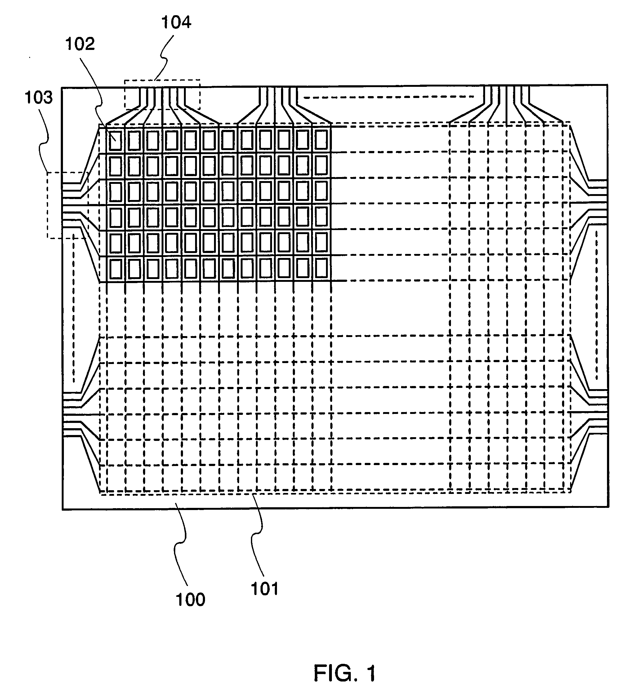
[0060]FIG. 4A shows a step of forming a gate electrode and a gate wiring connected to the gate electrode with a droplet discharge method over a substrate 100. Note that FIG. 4A shows a longitudinal sectional structure, and FIG. 13 shows a planar structure corresponding to A-B and C-D thereof.

[0061] In addition to a non-alkaline glass substrate such as barium borosilicate glass, alumino borosilicate glass, and aluminosilicate glass manufactured with a fusion method or a floating method, and a ceramic substrate, a plastic substrate having the heat resistance that can withstand processing temperature or the like can be used for the substrate 100. In addition, a semiconductor substrate such as single crystal silicon, a substrate in which a surface of a metal substrate such as stainless is provided with an insulatin...

embodiment mode 2

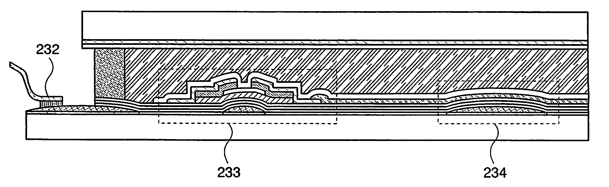
[0092] Embodiment mode 1 shows a structure in which a first electrode 224 and a wiring 220 connected to at least one of a source or a drain are connected directly; however, an insulating layer may be provided therebetween as another mode.

[0093] In this case, an insulating layer 240 functioning as a protective film is formed when the steps up to FIG. 5C is finished (see FIG. SA). A film to be formed of silicon nitride or silicon oxide formed by a sputtering method or a plasma CVD method may be applied to this protective film. It is necessary to form an opening 241 in the insulating layer 240, and the wiring 220 connected to at least one of the source and the drain is electrically connected to the first electrode 224 through the opening 241 (see FIG. 5B). At the time of forming the opening 241, an opening 242 necessary for attaching a connection terminal later may be simultaneously formed. A TFT substrate 200 is thus completed.

[0094] A method for forming the openings 241 and 242 is ...

embodiment mode 3

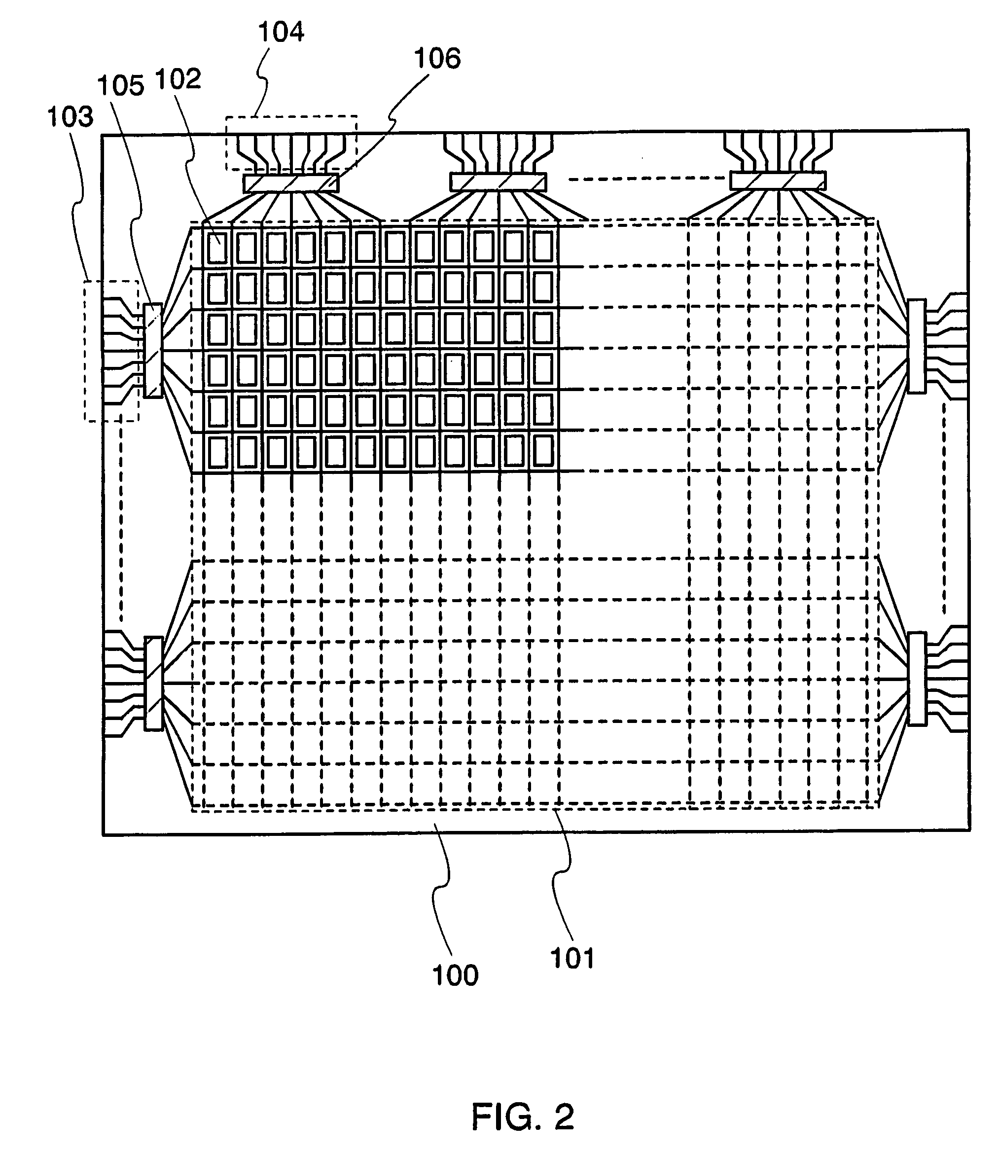
[0096] A method for manufacturing a channel etched type thin film transistor and a liquid crystal display device with the use thereof are explained in Embodiment Mode 3.

[0097] A wiring 202, a gate electrode 203, and a capacitor wiring 204 are formed over a substrate 100. These are formed by directly drawing a composition containing conductive substance over the substrate 100 with a droplet discharge method. Next, a gate insulating layer 207 is formed to have a single layer structure or a laminated structure by a plasma CVD method or a sputtering method. A specifically preferable mode is a lamination body of three layers of a first insulating layer 208 including silicon nitride, a second insulating layer 209 including silicon oxide, and a third insulating layer 210 including silicon nitride. Furthermore, a semiconductor layer 211 functioning as an active layer is formed. The above-mentioned steps are the same as those in Embodiment Mode 1.

[0098] An n-type semiconductor layer 301 is...


PUM

PropertyMeasurementUnit
sizeaaaaaaaaaa
sizeaaaaaaaaaa
sizeaaaaaaaaaa

Abstract

At least one or more of a conductive layer which forms a wiring or an electrode and a pattern necessary for manufacturing a display panel such as a mask for forming a predetermined pattern is formed by a method capable of selectively forming a pattern to manufacture a liquid crystal display device. A droplet discharge method capable of forming a predetermined pattern by selectively discharging a droplet of a composition in accordance with a particular object is used as a method capable of selectively forming a pattern in forming a conductive layer, an insulating layer, or the like.

Description

TECHNICAL FIELD [0001] The present invention relates to a display device to which an active element such as a transistor formed over a glass substrate is applied and to a method for manufacturing the same. BACKGROUND ART [0002] Conventionally, a display panel of a so-called active matrix driving method constituted by a thin film transistor (hereinafter also referred to as a “TFT”) over a glass substrate is known. As well as a manufacturing technique of a semiconductor integrated circuit, this display panel needs a step of patterning a thin film such as a conductor, a semiconductor, or an insulator by a light-exposure step using a photomask. [0003] A size of a mother glass substrate used for manufacturing a display panel is enlarged from 300 mm×400 mm of the first generation in the early 1990s to 680 mm×880 mm or 730 mm×920 mm of the fourth generation in 2000. Furthermore, the manufacturing technique made such a development that a number of display panels can be obtained from one sub...

Claims


Application Information

Patent Timeline
Patent Type & Authority Applications(United States)
IPC IPC(8): H01L29/04G02F1/1362G02F1/1368H01L21/336H01L21/768H01L21/77H01L21/84H01L27/12
CPCG02F1/1368G02F2001/136295H01L21/76838H01L27/12H01L29/66765Y10T428/24421H01L27/1292H01L33/08H01L2924/0002H01L27/1285H01L2924/00G02F1/136295H01L27/1214H01L29/4908
Inventor YAMAZAKI, SHUNPEIMAEKAWA, SHINJIFURUNO, MAKOTONAKAMURA, OSAMUIMAI, KEITARO
Owner SEMICON ENERGY LAB CO LTD
Why Eureka
Try Eureka