Charge coupled device with high quantum efficiency

a charge coupled, high-quantity technology, applied in the direction of radiation controlled devices, semiconductor devices, electrical devices, etc., can solve the problems of poor sensitivity of conventional ccds to short wavelength bands such as blue, uv, soft x-ray, and poor yield, and achieve high quantum efficiency (qe), facilitate high charge transfer efficiency, and high cte

Inactive Publication Date: 2007-03-08
IMAGERLABS
View PDF9 Cites 2 Cited by
  • Summary
  • Abstract
  • Description
  • Claims
  • Application Information

AI Technical Summary

Benefits of technology

[0014] One aspect of the present invention discloses a six-phase Front Illuminated Charge Coupled Device (CCD) pixel with a channel potential gradient and a window through which a wide band of photons can be sensed by the photosensitive silicon of the CCD, thus providing very high quantum Efficiency (QE) similar to the back thinned CCD without the concomitant yield and cost problems. The window is formed via commonly available fabrication process etch steps. Employing selective etch steps allows the removal of the layers residing on the top of the photosensitive silicon, such as the glass protective layer, the oxide gate insulating layer, the conductive gate layer such as polysilicon, and inter-metal dielectrics, without distorting the geometry of the cell. An implant doping for providing channel potential gradient from high to low potential levels is created within the silicon beneath the window region to facilitate high charge transfer efficiency (i.e., high CTE) from pixel to pixel via the transfer gates. In addition, the window provides a self aligned mask for the implantation steps and thus prevents the formation of pockets (or wells) due to misalignments that decrease the charge transfer efficiency and causes non-uniformity problems as associated with prior art. Furthermore the window provides a flat region that can be covered with an anti-reflective (AR) coating layer, thus further increasing the QE.

Problems solved by technology

However conventional CCDs suffer from poor sensitivity to short wavelength bands such as blue, UV, and soft X-Ray.
This problem is caused by the absorption of short wavelength photons by the polysilicon layers utilized in forming gate structures in a CCD.
However, Back Thinned CCD is a costly process.
The process of thinning is both expensive and poor yielding which further increases the device price.
A disadvantage to this approach is that it suffers from non-uniformity caused by the variation of the ITO layer thickness across the sensor array that is due to chemical mechanical polishing (CMP) used for achieving the required electrical isolation between adjacent ITO gates.
Thus creating a potential pocket (or well) in the region beneath the electrode gap introduces charge transfer inefficiency.
However, CCD with U-shaped gates, while addressing the problems of CCD with ITO Gate, is afflicted by reduced full well due to much reduction in the gate area.
However, this approach suffers from increased pixel-to-pixel crosstalk due to scattered light emitted from the phosphor layer since there is a gap between the short wavelength sensitive coating, such as Lumagen and the silicon surface.
A drawback to this technology is that it also suffers from charge transfer efficiency (CTE) problems due to spurious potential pockets which trap charges in the signal transfer channel.
The potential pockets are the result of unavoidable small misalignment of implants for potential well shape.
Adding background charge in order to fill the pockets may increase CTE but inevitably increases noise (i.e., shot noise of the added background charge).
However, OPP CCD with dual-phase timing suffers from slow charge transfer process, thus precluding it from usage in applications where reasonable frame rates are of interest.
Since the transfer through the open phase is unaided by electric or fringing fields and controlled primarily through thermal diffusion for smaller charge packets, the CTE at higher speeds will be unacceptable for low signals, and poor for even larger packets that are helped by self induced drift.
In addition, the window provides a self aligned mask for the implantation steps and thus prevents the formation of pockets (or wells) due to misalignments that decrease the charge transfer efficiency and causes non-uniformity problems as associated with prior art.

Method used


Image

  • Charge coupled device with high quantum efficiency
  • Charge coupled device with high quantum efficiency
  • Charge coupled device with high quantum efficiency

Examples


Embodiment Construction

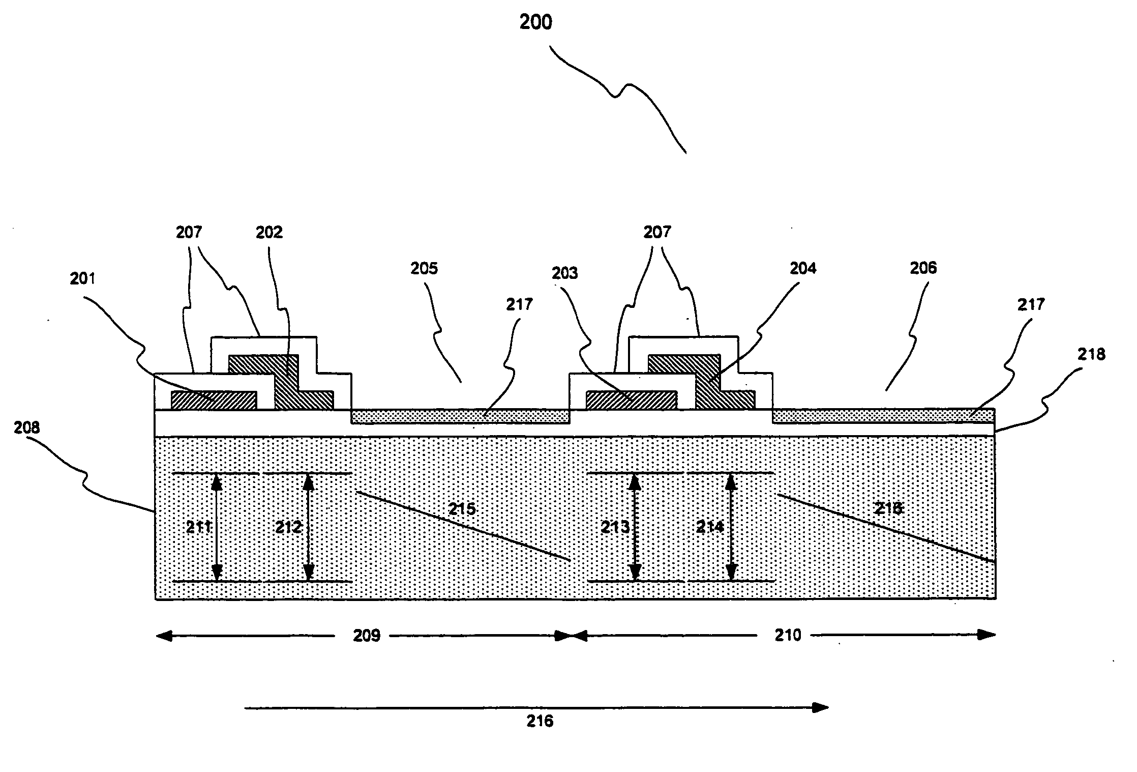
[0025]FIG. 1 provides a top view of a pixel-pair 100 of a six-phase front-illuminated CCD according to one embodiment of the present invention. The pixel-pair 100 comprises two cells 110 and 111 which accommodate charge transfer in a direction 112 from cell 110 to cell 111. A plurality of pixel-pairs 100 may form a CCD array with additional circuitry such as parallel and serial shift registers, charge amplification blocks and so on, as is known in the art. Pixel-pair 100 includes four independently controlled gates 101, 102, 103 and 104 that are formed from conductive material such as but not limited to polysilicon or transparent material such as indium-tin-oxide (ITO). The potential energy within the silicon regions is controlled by these gates via six-phase timing that will be further detailed in FIG. 3. Pixel-pair 100 further includes window regions 107 and 108 through which wide a band of photons can be sensed by the photosensitive silicon beneath it, thus providing very high QE...


PUM


Abstract

A six-phase charge coupled device (CCD) pixel includes a pixel pair, with each pixel having two adjacent control gates overlying corresponding variable potential wells, where voltages applied to the control gates enable charge to be accumulated into and transferred out of the wells. A clear window region overlies a fixed potential gradient region, decreasing in potential away from the control gates. This region enables a wide band of photons to be sensed by the photosensitive silicon of the CCD. The decreasing potential levels facilitate high charge transfer efficiency (i.e., high CTE) from pixel to pixel via the control or transfer gates. By applying particular voltages to the control gates, charge can be quickly and efficiently transferred between pixels. In addition, the window provides a self aligned mask for the implantation steps and thus prevents the formation of pockets (or wells) due to misalignments that decrease the charge transfer efficiency and causes non-uniformity problems as associated with prior art. Furthermore the window provides a flat region that can be covered with an anti-reflective (AR) coating layer, thus further increasing the quantum efficiency.

Description

RELATED APPLICATION [0001] The present application is based on and claims priority to U.S. Provisional application Ser. No. 60 / 714,129, filed Sep. 2, 2005 and bearing Attorney Docket No. M-16158-V1US.BACKGROUND [0002] 1. Field of the Invention [0003] The present invention relates to methods of manufacturing semiconductor devices, and more particularly to forming high quantum efficiency (QE) charge coupled devices (CCDs). [0004] 2. Related Art [0005] Charged coupled device (CCD) sensors have been utilized in various demanding sensing applications such as high end visible light imaging, UV imaging, X-Ray imaging, spectroscopy, and more. However conventional CCDs suffer from poor sensitivity to short wavelength bands such as blue, UV, and soft X-Ray. This problem is caused by the absorption of short wavelength photons by the polysilicon layers utilized in forming gate structures in a CCD. The poor sensitivity to certain wavelength bands is manifested as a reduction in the total Quantum...

Claims


Application Information

Patent Timeline
Patent Type & Authority Applications(United States)
IPC IPC(8): H01L29/76
CPCH01L27/1462H01L27/1485H01L27/14806H01L27/14683
Inventor WADSWORTH, MARK
Owner IMAGERLABS
Why Eureka
Try Eureka