
Organic transistor active substrate, manufacturing method thereof, and electrophoretic display

Active Publication Date: 2007-03-08
TRANSCEND OPTRONICS (YANGZHOU) CO LTD
View PDF6 Cites 29 Cited by
  • Summary
  • Abstract
  • Description
  • Claims
  • Application Information

AI Technical Summary

Benefits of technology

[0098] The present invention provides an organic transistor active substrate, an electrophoretic display, and a manufacturing method thereof in which one or more of the above-described disadvantages are eliminated.
[0101] According to one embodiment of the present invention, it is possible to manufacture an active substrate including an organic TFT that can be entirely manufactured by printing processes, so that costs of the manufacturing operation and the manufacturing device can be reduced. Further, the electrophoretic display can be manufactured at low cost.

Problems solved by technology

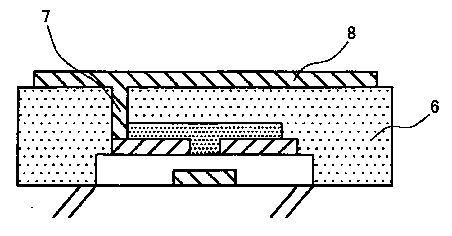
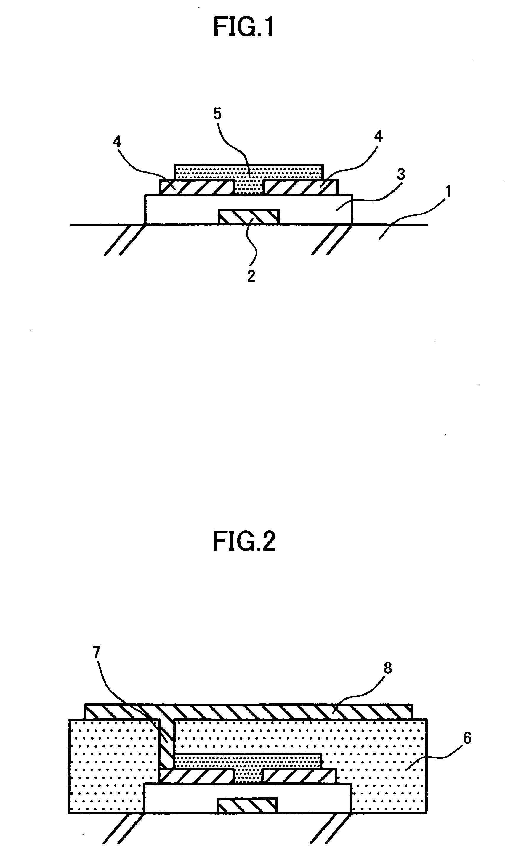
However, properties of the organic TFT may deteriorate when forming the interlayer insulating film 6 or subsequently forming a through-hole 7.
not simple process, plasma damage occurs
First, methods of forming the a) inorganic insulating film and their problems are described.
(1) Inconvenience of using a vacuum device
(2) The sample is exposed to an environment including positive charges and negative charges, which electrically damage the sample (generally referred to as plasma damage).
Particularly, failures occur when forming an interlayer insulating layer on the transistor.
Examples of the failures include drifting of the threshold voltage of the transistor and a decline in the insulating resistance value of the gate insulating film.
However, in this film formation method, tetraethoxysilane is subject to hydrolytic cleavage, polycondensation, and dehydration reaction; therefore, heat treatment of 200° C. is required (heat treatment of 400° C. is required in the case of withdrawal of residual water group).
Accordingly, this method cannot be employed when the substrate is made of a material such as plastic, which restricts the heat treatment temperature.
However, when forming an organic insulating film, there is a problem in that an organic solvent included in photoresist elutes the base insulating film.
When the etching is done by a dry process, plasma damage is incurred by the TFT.
Similar to the above example, the bias electric field also causes drifting of the transistor performance and deterioration of breakdown resistance of the gate insulating film, thereby causing plasma damage.
Thus, even with the cast film formation method using an organic insulating film, the results are unsatisfactory.
A stainless mesh is provided at the emulsion aperture, which hampers the passage of ink.
This leveling operation has a detrimental effect in terms of reproducing dimensions of the pattern.
Accordingly, screen printing has not been conventionally employed for printing interlayer insulating films, although the method is simple.
Thus, the organic solvent included in the interlayer film ink (hereinafter, simply referred to as “paste”) dissolves or swells the organic semiconductor layer, which may result in degraded semiconductor properties.
When the inkjet method is employed for forming a wiring pattern, the dimensions of the pattern are restricted by the volume of ejected ink and landing accuracy of ink.
However, the conventional method is performed in subsequent processes to form the interlayer insulating film (second insulating film) 6, to open the contact hole, and to form the individual electrode 8 shown in FIG. 2; therefore, costs are not thoroughly reduced.
In intaglio printing, it is possible to print patterns with line widths of 20 μm, so that the resolution is sufficient; however, intaglio printing is inappropriate for forming thin films (the film thickness is generally 2 to 3 μm in intaglio printing).
The aforementioned intaglio printing and relief printing methods do not satisfy the requirement of positional alignment.
This may cause the operating point of the transistor to shift.
With the intaglio printing method, thick films can be formed; however the printing positions cannot be sufficiently aligned with respect to the base pattern.

Method used


Image

  • Organic transistor active substrate, manufacturing method thereof, and electrophoretic display
  • Organic transistor active substrate, manufacturing method thereof, and electrophoretic display
  • Organic transistor active substrate, manufacturing method thereof, and electrophoretic display

Examples


example 1

[0117] (1) Formation of Organic Transistor

[0118] Commercially available nano-silver ink was used to print a desired pattern on a glass substrate by using an inkjet device manufactured by Ricoh Printing Systems, Ltd. The pattern was heat treated at 200° C. to form the first electrode.

[0119] Next, thermal polymerization type polyimide was coated as the first insulating film by spin coating, and heat treated at 280° C. Subsequently, ultraviolet rays were irradiated to desired parts (where second electrodes are to be formed, described later) via a photomask, to modify the surface. The superposition accuracy of the photomask on the first electrode pattern was calculated, and the shift amount was within ±10 μm with respect to the total pitch of 200 mm.

[0120] Next, similar to the formation of the first electrode, nano-silver ink was used in an IJ method to form the second electrodes. The exposure part cannot recognize the pattern by CCD observation. Accordingly, the substrate was matche...

example 2

[0131] The electrophoretic display according to an embodiment of the present invention has the structure as shown in FIG. 4. Specifically, the supporting substrate 11 is disposed on the transparent electrode (ITO: Indium Tin Oxide) 10 as a common electrode. The electrophoretic microcapsules 9 for displaying black / white are sandwiched between the transparent electrode 10 and the third electrode 8 (individual electrode, pixel electrode) of the organic transistor active substrate formed by the method described in example 1. It was observed that the color displayed by the pixel change between black and white by applying a voltage of −20 V to the scanning line and applying a voltage of ±20 V to the (pixel) signal line. The electrophoretic microcapsules 9 are medium that can display black and white, and each capsule includes white particles, black particles and an insulating solvent.

[0132] The method of manufacturing the electrophoretic display is described in detail.

[0133] Titanium oxi...


PUM


Abstract

A method of manufacturing an organic transistor active substrate is disclosed. The organic transistor active substrate includes an organic transistor in which a first electrode is formed on a substrate, a first insulating film is formed on the first electrode, a pair of second electrodes is formed on the first insulating film, and an active layer made of an organic semiconductor material is formed on the pair of second electrodes. The organic transistor is laminated with a second insulating film, and the second insulating film is laminated with a third electrode which is electrically coupled to one of the second electrodes via a through-hole provided through the second insulating film. The first electrode is formed by inkjet ejection; the first insulating film is formed by coating; the pair of second electrodes is formed by inkjet ejection; the active layer is formed by inkjet ejection; the second insulating film is formed by screen printing; and the third electrode is formed by screen printing.

Description

BACKGROUND OF THE INVENTION [0001] 1. Field of the Invention [0002] The present invention relates generally to active substrates using organic transistors, and more particularly to an organic transistor active substrate, a manufacturing method thereof, and an electrophoretic display using the organic transistor active substrate that can be manufactured by simple methods at low cost. [0003] 2. Description of the Related Art [0004] Conventionally, the following matrix type displays are known: passive type displays and active type displays. A passive type display is driven by a scanning electrode and a data electrode that are mutually orthogonal. An active type display selects pixels to be lit by using a switching element such as a transistor and a memory element. [0005] Examples of active type displays are disclosed in Japanese Laid-Open Patent Application No. 2003-255857 “Organic EL Display” (Patent Document 1), Japanese Laid-Open Patent Application No. 2003-318196 “Active element an...

Claims


Application Information

Patent Timeline
IPC IPC(8): G03G5/00
CPCH01L27/283H01L51/0022H01L51/0021H01L51/0005H10K19/10H10K71/135H10K71/60H10K71/611
Inventor AKIYAMA, YOSHIKAZUYAMAGA, TAKUMITANO, TAKANORITOMONO, HIDENORIMURAKAMI, AKISHIGEARITA, HITOSHIARAUMI, MAYUKA
Owner TRANSCEND OPTRONICS (YANGZHOU) CO LTD
Learn More