Method of manufacturing a semiconductor device

a semiconductor device and manufacturing method technology, applied in the field of resist compounds, can solve the problems of reducing product yield, deteriorating transistor characteristics, difficult control of pattern dimension, etc., and achieve the effects of high heat resistance, high sensitivity, and high resolution

Inactive Publication Date: 2007-03-15
MITSUBISHI GAS CHEM CO INC
View PDF2 Cites 46 Cited by
  • Summary
  • Abstract
  • Description
  • Claims
  • Application Information

AI Technical Summary

Benefits of technology

[0007] An object of the present invention is to provide compounds which are sensitive to radiations such as excimer lasers from KrF, extreme ultraviolet rays (EUV), electron beams and X-rays, and provide radiation sensitive compositions containing such compounds. Another object of the present invention is to provide a simple method of producing non-polymeric radiation sensitive compositions that exhibit a high sensitivity, a high resolution, a high heat resistance, a high etching resistance and a good solubility in solvent.

Problems solved by technology

Therefore, in a finer lithographic process using the polymeric resist materials, the surface of patterns is roughened to make it difficult to control the dimension of patterns, thereby reducing product yields and deteriorating transistor characteristics.
Thus, the conventional lithographic techniques using the known polymeric resist materials cannot be applied to the production of fine patterns of 0.06 μm line width or smaller.
The resist materials (4) are less practicable because a complicated production process is required and the distortion of patterned images due to their low heat resistance occurs during the heat treatment after exposure to light (“Proceedings of SPIE”, vol.
The resist materials (6) are less practicable because a complicated production process is required, the raw materials are expensive, and metal catalysts unfavorable for the semiconductor production are used.
The resist materials (7) are less practicable because the distortion of patterned images due to their low heat resistance is likely to occur during the heat treatment after exposure to light and the adhesion to substrates is poor (JP 2002-328466A).
Since known resist compositions contain resin, the resist patterns formed therefrom has a large line edge roughness to make the compositions insufficient for practical use.
In addition, the compositions containing known resist compounds as the main component involve at least one of the following problems: the film-forming properties are poor because of a high crystallinity; the heat resistance is low to withstand semiconductor process; the compositions are sparingly soluble in safety solvents such as propylene glycol monoethyl ether acetate and ethyl lactate which are acceptable for use in semiconductor factory; and the adhesion to substrate is insufficient.
Therefore, known resist compounds are not suitable for single use.

Method used


Image

  • Method of manufacturing a semiconductor device
  • Method of manufacturing a semiconductor device
  • Method of manufacturing a semiconductor device

Examples


example 1

Synthesis of Compound 5-1

[0103]

(1) Synthesis of 1-(2-naphthyl)-1,1-bis(3-methyl-4-hydroxyphenyl)ethane

[0104] Into a solution prepared by heating a mixture of 43.2 g (0.4 mol) of o-cresol (reagent available from Kanto Chemical Co., Inc.) and 17.1 g (0.1 mol) of β-acetonaphthone (reagent available from Kanto Chemical Co., Inc.) to about 30° C., were added 0.1 ml of sulfuric acid, 0.8 ml of 3-mercaptopropionic acid and 10 ml of toluene. The reaction was allowed to proceed under stirring. After confirming that the conversion reached 100% by gas chromatography, 100 ml of toluene was added. After cooling, the precipitated solid was separated by vacuum filtration, washed with warm water of 60° C. under stirring and purified by silica gel column chromatography, to obtain 24 g of the titled compound.

(2) Synthesis of Compound 5-1

[0105] Into a solution prepared by mixing 1.84 g (5 mmol) of 1-(2-naphthyl)-1,1-bis(3-methyl-4-hydroxyphenyl)ethane synthesized above with 5 ml of anhydrous acet...

example 2

Synthesis of Compound 5-2

[0106]

[0107] Into a solution prepared by mixing 1.84 g (5 mmol) of 1-(2-naphthyl)-1,1-bis(3-methyl-4-hydroxyphenyl)ethane synthesized in Example 1 with 5 ml of anhydrous acetone and 1.2 mg of dimethylaminopyridine, 1.32 g (6 mmol) of di-tert-butyl dicarbonate was added dropwise over 10 min. The resultant mixture was stirred for 24 h at 40° C. The reaction liquid was purified by a silica gel column chromatography (eluent: ethyl acetate / hexane=1 / 3) to obtain the titled compound. The structure of the compound was determined by elemental analysis and 1H-NMR measurement. The results of the analysis are shown in Tables 1 and 2.

example 3

Synthesis of Compound 5-3

[0108]

(1) Synthesis of Biscatechol Compound

[0109] In the same manner as in Example 1(1) except for using 44.0 g (0.4 mol) of catechol (reagent available from Kanto Chemical Co., Inc.) in place of 43.2 g (0.4 mol) of o-cresol, 1-(2-naphthyl)-1,1-bis(3,4-dihydroxyphenyl)ethane was synthesized.

(2) Synthesis of Compound 5-3

[0110] Into a solution prepared by mixing 1.84 g (5 mmol) of 1-(2-naphthyl)-1,1-bis(3,4-dihydroxyphenyl)ethane synthesized above with 5 ml of anhydrous acetone and 1.2 mg of dimethylaminopyridine, 5.28 g (24 mmol) of di-tert-butyl dicarbonate was added dropwise over 10 min. The resultant mixture was stirred for 24 h at 40° C. The reaction liquid was poured into an excessive amount of water to precipitate solid matters. The obtained white powder was washed with distilled water three times, filtered under suction, and dried under reduced pressure, to obtain the titled compound. The structure of the compound was determined by elemental analy...


PUM

PropertyMeasurementUnit
widthaaaaaaaaaa
molecular weight distributionsaaaaaaaaaa
widthaaaaaaaaaa

Abstract

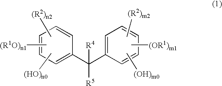
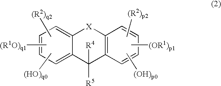
The compound of the present invention is represented by the following formula 1: wherein R1, R2, R4, R5, m0 to m2, and n0 to n2 are as defined in the description. Radiation sensitive compositions containing the compound of the formula 1 as a main component of the solid component are excellent in sensitivity, resolution, heat resistance, etching resistance, and solubility in solvent.

Description

TECHNICAL FIELD [0001] The present invention relates to resist compounds useful as acid-amplified non-polymeric resist materials, which have specific chemical structures. The present invention also relates to radiation sensitive compositions comprising such a compound and an acid generator. The resist compounds of the present invention are used as radiation sensitive materials for forming masks, etc. in the production of electronics parts such as LSI and VLSI, which are sensitive to radiations such as ultraviolet rays, far ultraviolet rays, extreme ultraviolet rays (EUV), electron beams and X-rays. BACKGROUND ART [0002] Conventionally known resist materials are generally polymeric materials capable of forming amorphous thin film. For example, a solution of polyhydroxystyrene derivative in a solvent is applied on a substrate to form a thin resist film, which is then irradiated with ultraviolet rays, far ultraviolet rays, electron beams, X-rays, etc., to form line patterns having a li...

Claims


Application Information

Patent Timeline
Patent Type & Authority Applications(United States)
IPC IPC(8): G03C1/00C07D311/82G03F7/039
CPCC07D311/82G03F7/0392G03F7/0045
Inventor OGURO, DAIECHIGO, MASATOSHI
Owner MITSUBISHI GAS CHEM CO INC
Why Eureka
Try Eureka