[0010] The present invention was made in view of the above and an object thereof is to realize the following when a substrate with an oxide film having been formed thereon is subjected to a nitridation process by
plasma generated by a microwave: that is, reducing damage at the time of the nitridation to eliminate a need for a subsequent annealing process or allowing the annealing process, even if performed, to be a weak annealing process, leading to improved quality of an oxynitride film, thereby achieving a reduced leakage current, an improved operating speed, improved NBTI resistance, and an improved static characteristic in a
semiconductor device.
[0012] According to the findings of the inventors, it is thought that in the case of the intermittent supply of the microwave for a
plasma nitridation process,
electron temperature of plasma decreases in an
OFF time of the supply of the microwave, and
ion bombardment to a surface of the oxide film is reduced, so that a
diffusion velocity of nitrogen active species in the oxide film is lowered, compared with the conventional case of the continuous supply of the microwave for the
plasma nitridation process. As a result, it is possible to prevent nitrogen from diffusing in an interface between, for example, a
silicon substrate and an oxynitride insulation film to make the concentration of nitrogen in the interface higher. As a result, it is possible to reduce a leakage current and form a higher-quality oxynitride film with an improved NBTI characteristic, without increasing the film thickness (
equivalent oxide thickness: EOT). The inventors have verified that NBTI resistance that is two to ten times as high as conventional NBTI resistance is achieved.
[0013] The inventors have further found that by changing at least a cycle of repetition of the supply and stop of the microwave or a ratio of an ON time and an
OFF time of the supply of the microwave (duty ratio) in the intermittent supply, it is possible to improve in a
MOSFET both an ON current characteristic and NBTI resistance which have been in a trade-off relation even if nitrogen concentration in a conventional film is changed. Therefore, when the microwave is supplied intermittently as described above, by changing at least the repetition cycle or the ratio of the ON time and the
OFF time of the supply of the microwave, it is possible to improve both the ON current characteristic and the NBTI resistance, whereby it is possible to improve film quality of an insulation film.
[0015]
Nitrogen concentration in the oxide film that has undergone the nitridation process is preferably 5 at % to 15 at %, more preferably 9 at % to 13 at %. Controlling the concentration within this range makes it possible to improve a leakage current, an ON current, and NBTI resistance. Further, a pressure in a process vessel during the nitridation process is preferably about 1 mTorr to 10 T (0.133 Pa to 1330 Pa). More preferably, the pressure is 10 mTorr to 1 T (1.33 Pa to 133.3 Pa).
[0016] For carrying out such
plasma processing of the present invention, a
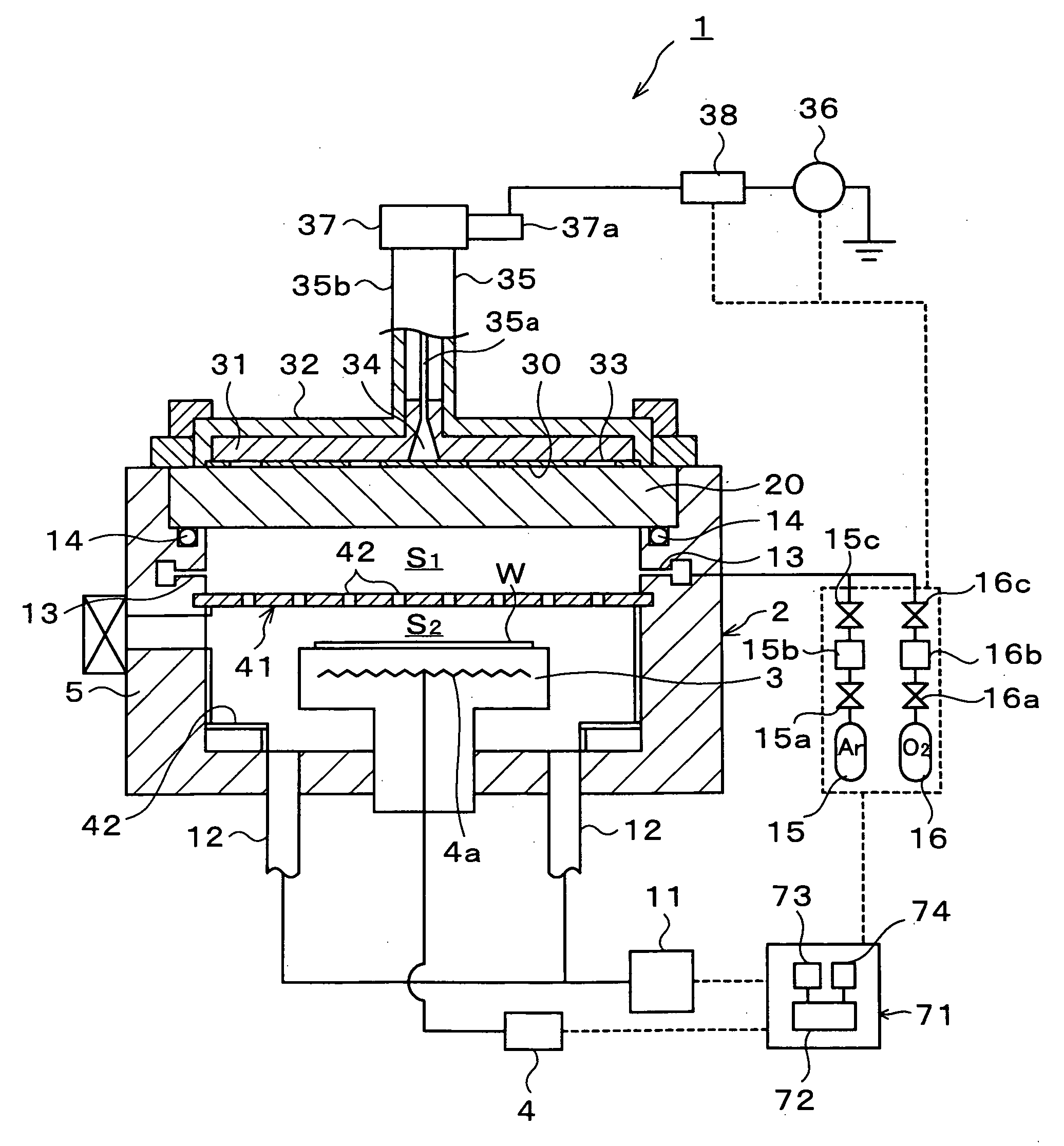
plasma processing apparatus having the following structure is preferably used. That is, the
plasma processing apparatus includes: a mounting table provided in a process vessel to
mount a substrate thereon; a
dielectric that is disposed in an upper area of the process vessel and through which the microwave is introduced into a process space to generate the plasma; a
gas supply part supplying a process gas to an upper area in the process vessel; and a
dielectric plate that is disposed at a position lower than a
gas supply port of the
gas supply part and higher than the substrate placed on the mounting table, has a large number of through holes, and covers at least the substrate, and by using the plasma
processing apparatus when the
plasma nitridation process is performed, high-energy ions are intercepted by the
dielectric plate having a large number of the through holes, so that it is possible to alleviate damage to a
nitride film and reduce plasma damage accompanying the plasma nitridation process. Consequently, an annealing process that is thereafter performed for damage
recovery can be a weak annealing process that anneals the substrate in a shorter time, and accordingly an increase in film thickness during the annealing process is reduced.
[0018] According to the present invention, when a substrate with an oxide film having been formed thereon is subjected to a nitridation process by plasma generated by a microwave, damage at the time of the plasma nitridation is reduced and a need for a subsequent annealing process is eliminated, or the annealing process, even if performed, may be a weak annealing process. Consequently, it is possible to improve quality of an oxynitride film to realize a reduced leakage current, an improved operating speed, and improved NBTI resistance of a manufactured
semiconductor device.

