These electronic devices have been traditionally fabricated using
silicon (Si) as a light-absorbing, semiconducting material in a relatively expensive production process.
A central challenge in cost-effectively constructing a large-area CIGS-based
solar cell or module is that the elements of the CIGS layer must be within a narrow stoichiometric ratio on nano-, meso-, and macroscopic
length scale in all three dimensions in order for the resulting
cell or module to be highly efficient.
Achieving precise
stoichiometric composition over relatively large substrate areas is however difficult using traditional vacuum-based deposition processes.
For example, it is difficult to deposit compounds and / or alloys containing more than one element by
sputtering or
evaporation.
Both techniques rely on deposition approaches that are limited to line-of-
sight and limited-area sources, tending to result in poor surface coverage.
Line-of-
sight trajectories and limited-area sources can result in non-uniform three-dimensional distribution of the elements in all three dimensions and / or poor film-thickness uniformity over large areas.
Such non-uniformity also alters the local stoichiometric ratios of the absorber layer, decreasing the potential power conversion efficiency of the complete
cell or module.
However, solar cells fabricated from the sintered
layers had very low efficiencies because the structural and electronic quality of these absorbers was poor.
A difficulty in this approach was finding an appropriate fluxing agent for dense CulnSe2 film formation.
Solar cells made in this manner also had poor conversion efficiencies.
Porous
solar cell absorbers yield unstable devices because of the large internal surface area within the device, and small grains limit the conversion efficiency of solar cells.
Another key limitation of this method was the inability to effectively incorporate
gallium into the material.
The absence of
gallium decreases the potential power conversion efficiency of the
solar cell.
In practice, while
gallium oxide particles can easily be produced, it is very difficult to reduce
gallium oxide, even at relatively high temperatures, and in the absence of reduction,
gallium oxide cannot be effectively used as a precursor material for gallium in the final film.
Accordingly, in addition to poor stability, solar cells made using the approach of Basol et al. had sub-optimal power conversion efficiency.
A
disadvantage of solar
cell devices comprised of thin-film absorber
layers formed in this manner was the poor reproducibility of the resulting device performance, and the porous form of the absorber layer, which tends to result in poor device stability.
However, a means to incorporate additional Ga beyond that possible through a
solid-solution (containing either Cu+Ga or In+Ga) restricts the potential performance of a device constructed by this method.
In particular, since the presence of additional gallium in the light absorbing film serves both to broaden the bandgap of the
semiconductor material and to increase the
open circuit voltage of the solar cell, a lack of additional gallium in the light-absorbing thin film tends to decrease the potential power conversion efficiency of solar cells created in this manner.
However, no technique was known in the prior art to create gallium
nanoparticle powders sufficient and adequate for
semiconductor applications, in part because gallium is molten at
room temperature and therefore does not lend itself to common techniques for creating nanoparticles in the form of powders that are then dispersed in solution (as commonly done with the other elements).
As a result, it was not possible in the prior art to directly incorporate gallium (or incorporate gallium in a high percentage) into the metallic dispersion used to print the CIG precursor of a CIGS solar cell.
In particular, non-uniformities can arise from the formation of more than one
single phase when preparing the CIG precursor layer with the composition required for a high-efficiency thin-film CIGS solar cell or module.
Rapid thermal processing such a non-uniform CIG precursor layer in the presence of VIA sources can result in both lateral non-uniformity of the final CIGS, and (large) CIS crystals at the front whereas the back mainly contains (small) Ga-rich CIGS crystals.
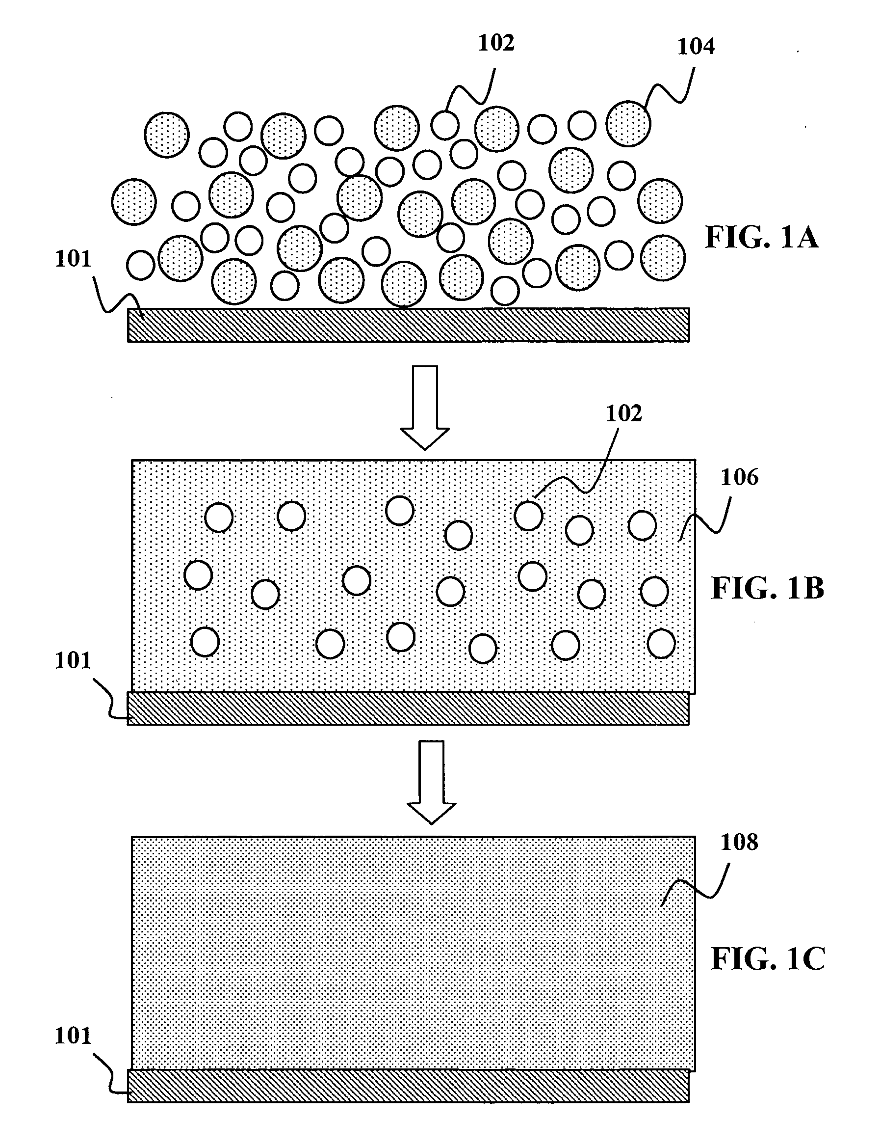
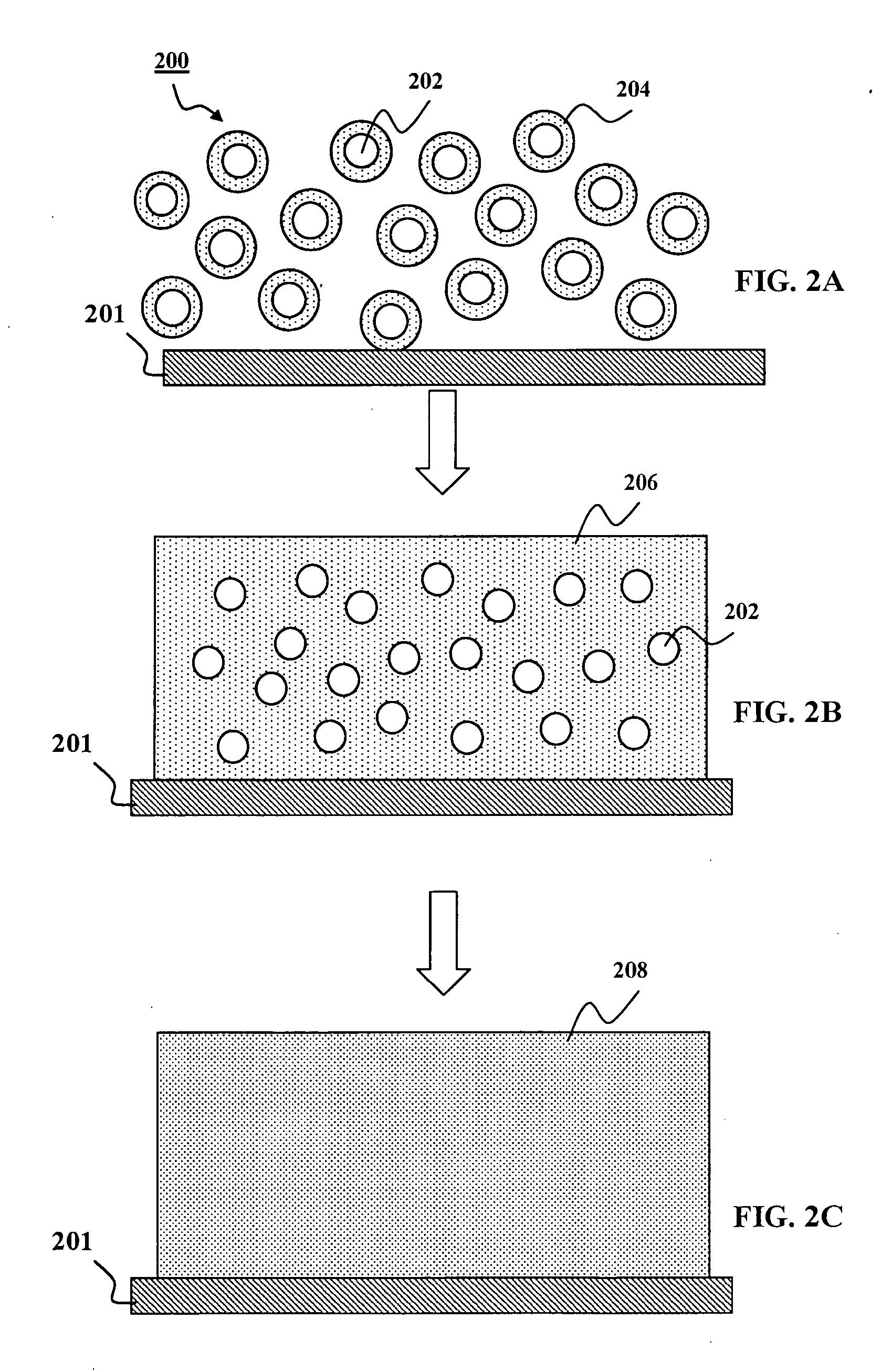
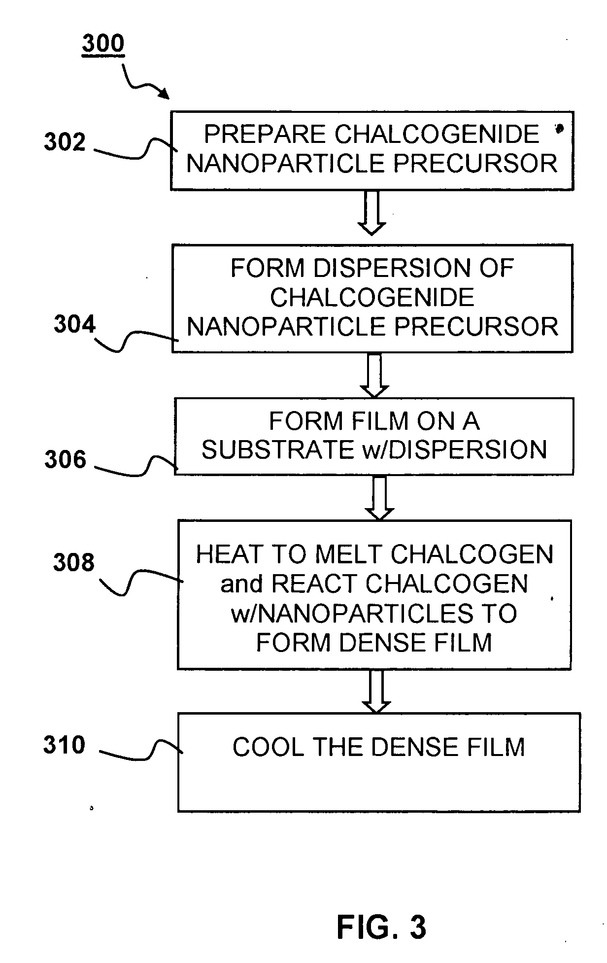
So far, no promising results have been obtained when using chalcogenide powders for fast
processing to form CIGS thin-films suitable for solar cells.
Due to high temperatures and / or long
processing times required for
sintering, formation of a IB-IIIA-chalcogenide compound film suitable for thin-film solar cells is challenging when starting from IB-IIIA-chalcogenide powders where each individual particle contains appreciable amounts of all IB, IIIA, and VIA elements involved, typically close to the
stoichiometry of the final IB-IIIA-chalcogenide compound film.
In particular, due to the limited contact area between the
solid powders in the layer and the high melting points of these ternary and quarternary materials,
sintering of such deposited
layers of powders either at high temperatures or for extremely long times provides ample energy and time for phase separation, leading to poor compositional uniformity of the CIGS absorber layer at multiple spatial scales.
Poor uniformity was evident by a wide range of heterogeneous layer features, including but not limited to
porous layer structure, voids, gaps,
cracking, and regions of relatively low-density.
This non-uniformity is exacerbated by the complicated sequence of phase transformations undergone during the formation of CIGS crystals from precursor materials.
In particular, multiple phases forming in discrete areas of the nascent absorber film will also lead to increased non-uniformity and ultimately poor device performance.
The requirement for fast
processing then leads to the use of high temperatures, which would damage temperature-sensitive foils used in roll-to-roll processing.
Indeed, temperature-sensitive substrates limit the
maximum temperature that can be used for processing a precursor layer into CIS or CIGS to a level that is typically well below the
melting point of the ternary or quarternary
selenide (>900° C.).
Both time and temperature restrictions, therefore, have not yet resulted in promising results on suitable substrates using ternary or
quaternary selenides as starting materials.

